Figure 3
Download original image
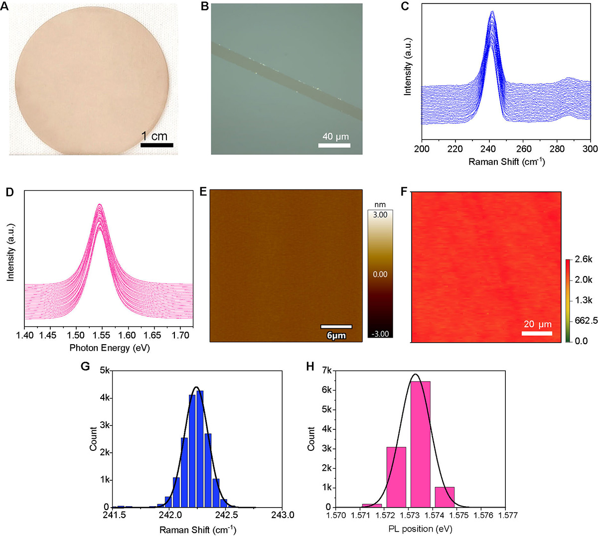
Wafer-scale MoSe2 single crystals. (A) Photograph of 2-inch monolayer MoSe2 single-crystal film on C/A-1° sapphire substrate. (B) Optical microscopy image showing the cleanness, uniformity, and continuity of the as-grown MoSe2 film. A scratch was made for the optical contrast. (C, D) Raman and PL line scans across a 2-inch MoSe2 single-crystal film. (E) AFM height image of as-grown MoSe2 film, displaying a clean and wrinkle-free surface. (F) SHG mapping over 100 μm×100 μm, revealing the single-crystal feature of the as-grown MoSe2 film. (G, H) Statistical distributions of the Raman and PL peak position from three mapping zones (16875 Raman spectra, 10800 PL spectra).
Current usage metrics show cumulative count of Article Views (full-text article views including HTML views, PDF and ePub downloads, according to the available data) and Abstracts Views on Vision4Press platform.
Data correspond to usage on the plateform after 2015. The current usage metrics is available 48-96 hours after online publication and is updated daily on week days.
Initial download of the metrics may take a while.