Figure 3
Download original image
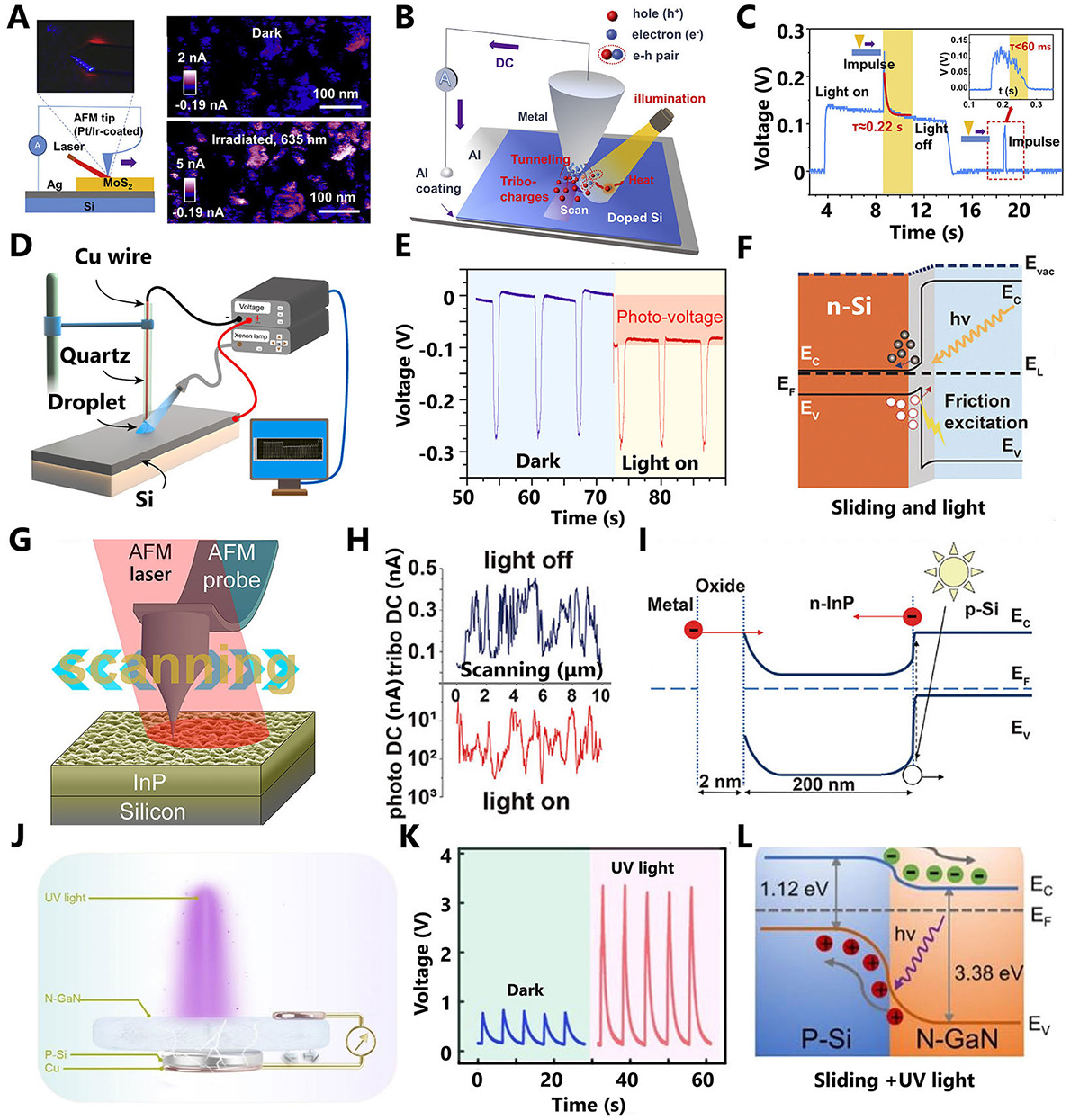
TVNG based on traditional semiconductor materials. (A)‒(C) Schematic diagram of metal/silicon point contact system structure. Adapted with permission from Ref. [38], Copyright©2019, Elsevier. (D)‒(F) Schematic diagram of interface diagram of DI water and Si crystal. Adapted with permission from Ref. [31]. Copyright©2021, Elsevier. (G)‒(I) Schematic diagram of metal-oxide-semiconductor interface. Adapted with permission from Ref. [39]. Copyright©2019, American Chemical Society. (J)‒(L) Schematic diagram of nGaN and pSi interface. Adapted with permission from Ref. [40]. Copyright©2021, American Chemical Society.
Current usage metrics show cumulative count of Article Views (full-text article views including HTML views, PDF and ePub downloads, according to the available data) and Abstracts Views on Vision4Press platform.
Data correspond to usage on the plateform after 2015. The current usage metrics is available 48-96 hours after online publication and is updated daily on week days.
Initial download of the metrics may take a while.