| Issue |
Natl Sci Open
Volume 5, Number 3, 2026
|
|
|---|---|---|
| Article Number | 20260023 | |
| Number of page(s) | 3 | |
| Section | Materials Science | |
| DOI | https://doi.org/10.1360/nso/20260023 | |
| Published online | 10 March 2026 | |
COMMENTARY
Fibre integrated circuits towards intelligent wearable electronics
1
State Key Laboratory of Catalysis, Dalian Institute of Chemical Physics, Chinese Academy of Sciences, Dalian 116023, China
2
University of Chinese Academy of Sciences, Beijing 100049, China
3
Dalian National Laboratory for Clean Energy, Chinese Academy of Sciences, Dalian 116023, China
* Corresponding authors (emails: This email address is being protected from spambots. You need JavaScript enabled to view it.
(Xiaoyu Shi); This email address is being protected from spambots. You need JavaScript enabled to view it.
(Zhong-Shuai Wu))
Received:
14
February
2026
Accepted:
6
March
2026
The advancement of wearable electronics is accelerating the evolution of devices toward multifunctionality and system-level integration [1]. Current fibre devices already demonstrated multiple discrete functions, such as energy harvesting and storage, sensing, and display, thereby laying a foundation for future intelligent wearable platforms [2]. Nevertheless, the essential signal processing components in such a system still depend on externally connected rigid silicon-based chips. This limitation fundamentally contradicts the flexible and conformal nature of fibres and severely impedes the realization of truly integrated smart fibre systems [3,4]. The critical bottleneck stems from the intrinsic curved geometry and limited surface area of fibres, which hinder the high-resolution fabrication of dense, multifunctional circuits necessary for on-fibre information processing.
Recently, a breakthrough by Peng’s group published in Nature has addressed this fundamental challenge [5]. The authors developed a transformative fibre integrated circuit (FIC) based on a multilayer spiral architecture, fabricated through an innovative strategy combining high-precision patterning on a flat elastic polymer substrate with a modified rolling process that transformed the planar circuits into a fibre geometry. By fully utilizing the radial dimension, this architecture achieved an extraordinary integration density of 105 transistors per centimeter, thereby enabling standalone signal processing and computing functions within a single fibre.
As a representative demonstration, the authors fabricated a 300-μm-diametre FIC incorporating logic circuits. Microscopic imaging confirmed uniform and well-defined circuit patterns with linewidths as narrow as to 5 μm (Figure 1a). Fluorescence tomography further visualized the internal multilayered architecture, revealing spirally arranged layers along the radial direction, with circuits wrapping 360° around the circumference to form a three-dimensional interconnection network (Figure 1b, c). Notably, this fabrication strategy exhibited remarkable scalability, allowing for the production of metre-long FICs with preciously tunable diameters through adjustments in substrate dimensions and layer thicknesses (Figure 1d, e).
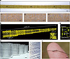 |
Figure 1 Photographs showing the structure of FICs. (a) Photograph of a FIC with exclusive-or circuits on the fibre surface (scale bar: 200 μm) and enlarged views (scale bars: 40 μm). (1), (2) and (3) show the uniformity of the circuits in the FIC. (b) Reconstructed three-dimensional fluorescence photomicrograph showing the connectivity of the microdevices in a FIC. The circuit can be distributed 360° around the fibre circumference. (c) Fluorescence photomicrograph showing an active driving circuit unit inside a FIC, suggesting that a wide variety of devices can be integrated into the fibre. Scale bar: 40 μm. (d) Photograph of FICs being produced at a large scale. The enlarged photograph shows the continuity of circuits in the FICs. Scale bars: 1 cm (left); 1 mm (right). (e) Photograph of a FIC being knotted and placed on a thumb, exhibiting the flexibility and structural integrity of the FIC. Scale bar: 2 mm. Reproduced with permission from Ref. [5]. |
Furthermore, the FIC demonstrated outstanding flexibility and durability that are unattainable with conventional rigid chips, attributed to its innovative modulus-graded heterostructure design. This architecture alternated high-modulus parylene buffer layers with soft polydimethylsiloxane interlayer, effectively dissipating and redistributing external stress. Consequently, the FIC withstood extreme mechanical deformations, including compression under a 15.6-ton truck, 10000 cycles of bending and abrasion, 30% stretching, and twisting up to 180° cm−1.
Functionally, the FIC executed digital and analogue computational tasks on par with commercial silicon-based chips, such as logic gates, sequential circuits, and waveform generators. Beyond these standard operations, the incorporation of organic electrochemical transistors enabled neuromorphic computing, achieving a recognition accuracy of 99.8% on standard image‑classification tasks. Further, the authors realized fully integrated closed-loop systems that incorporated power supply, sensing, data processing, and display modules within a single fibre, yielding self‑sufficient intelligent fibre prototypes. These advanced capabilities underpinned several transformative applications, including high-density neural probes featuring in-situ signal amplification for high-fidelity recording, smart textiles woven embedded with pixel-level addressable displays, and machine-washable tactile gloves capable of programmable haptic feedback.
Overall, this work represents a paradigm shift in fibre electronics, transforming fibres from passive functional carriers into intelligent platforms endowed with autonomous information processing capabilities. By serving as a versatile and robust computational core, the FIC addresses a key missing link in realizing truly self-sufficient fibre-integrated systems. This advancement provides a foundational framework for next-generation wearable devices, implantable electronics, and human-machine interfaces, thereby propelling fibre electronics toward a new era of functional integration and system-level intelligence.
Conflict of interest
The authors declare no conflict of interest.
References
- Ren Z, Shi X, Yang E, et al. 3D-printed stretchable modular integrated microsystems toward sweat monitoring powered by wireless charging sodium-ion micro-batteries. Natl Sci Rev 2025; 12: nwaf364. [Article] [Google Scholar]
- Zeng K, Shi X, Tang C, et al. Design, fabrication and assembly considerations for electronic systems made of fibre devices. Nat Rev Mater 2023; 8: 552-561. [Article] [Google Scholar]
- Qian S, Liu M, Dou Y, et al. A ‘Moore’s law’ for fibers enables intelligent fabrics. Natl Sci Rev 2023; 10: nwac202. [Article] [Google Scholar]
- Loke G, Alain J, Yan W, et al. Computing fabrics. Matter 2020; 2: 786-788. [Article] [Google Scholar]
- Wang Z, Chen K, Shi X, et al. Fibre integrated circuits by a multilayered spiral architecture. Nature 2026; 650: 102-109. [Article] [Google Scholar]
© The Author(s) 2026. Published by Science Press and EDP Sciences.
 This is an Open Access article distributed under the terms of the Creative Commons Attribution License (https://creativecommons.org/licenses/by/4.0), which permits unrestricted use, distribution, and reproduction in any medium, provided the original work is properly cited.
All Figures
|
Figure 1 Photographs showing the structure of FICs. (a) Photograph of a FIC with exclusive-or circuits on the fibre surface (scale bar: 200 μm) and enlarged views (scale bars: 40 μm). (1), (2) and (3) show the uniformity of the circuits in the FIC. (b) Reconstructed three-dimensional fluorescence photomicrograph showing the connectivity of the microdevices in a FIC. The circuit can be distributed 360° around the fibre circumference. (c) Fluorescence photomicrograph showing an active driving circuit unit inside a FIC, suggesting that a wide variety of devices can be integrated into the fibre. Scale bar: 40 μm. (d) Photograph of FICs being produced at a large scale. The enlarged photograph shows the continuity of circuits in the FICs. Scale bars: 1 cm (left); 1 mm (right). (e) Photograph of a FIC being knotted and placed on a thumb, exhibiting the flexibility and structural integrity of the FIC. Scale bar: 2 mm. Reproduced with permission from Ref. [5]. |
| In the text | |
Current usage metrics show cumulative count of Article Views (full-text article views including HTML views, PDF and ePub downloads, according to the available data) and Abstracts Views on Vision4Press platform.
Data correspond to usage on the plateform after 2015. The current usage metrics is available 48-96 hours after online publication and is updated daily on week days.
Initial download of the metrics may take a while.