Figure 1
Download original image
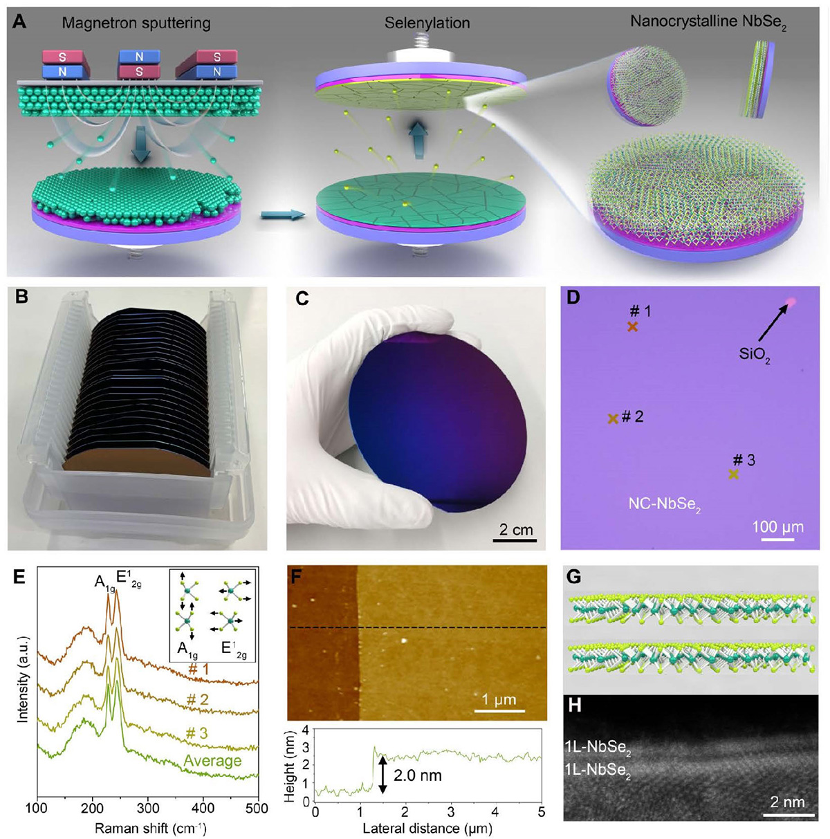
The batch growth of wafer-scale NC-NbSe2 films. (A) Schematic illustration of the two-step vapor deposition growth that involves a magnetron sputtering of Nb film and a subsequential selenylation into NC-NbSe2 film in a continuous preparation route. (B, C) Photographs and (D) optical microscopic image of as-grown NC-NbSe2 film on 4-inch SiO2/Si substrates. Notably, the SiO2 substrate was artificially exposed for visual guidance. (E) The representative Raman spectra of NC-NbSe2 film. The inset shows the characteristic Raman stretching modes of A1g and ![]() of NbSe2. (F) AFM image and the corresponding height profile of NC-NbSe2 films directly grown on SiO2/Si. (G) Atomic structure model and (H) the ADF-STEM image of bilayer NC-NbSe2 film.
of NbSe2. (F) AFM image and the corresponding height profile of NC-NbSe2 films directly grown on SiO2/Si. (G) Atomic structure model and (H) the ADF-STEM image of bilayer NC-NbSe2 film.
Current usage metrics show cumulative count of Article Views (full-text article views including HTML views, PDF and ePub downloads, according to the available data) and Abstracts Views on Vision4Press platform.
Data correspond to usage on the plateform after 2015. The current usage metrics is available 48-96 hours after online publication and is updated daily on week days.
Initial download of the metrics may take a while.