Figure 2
Download original image
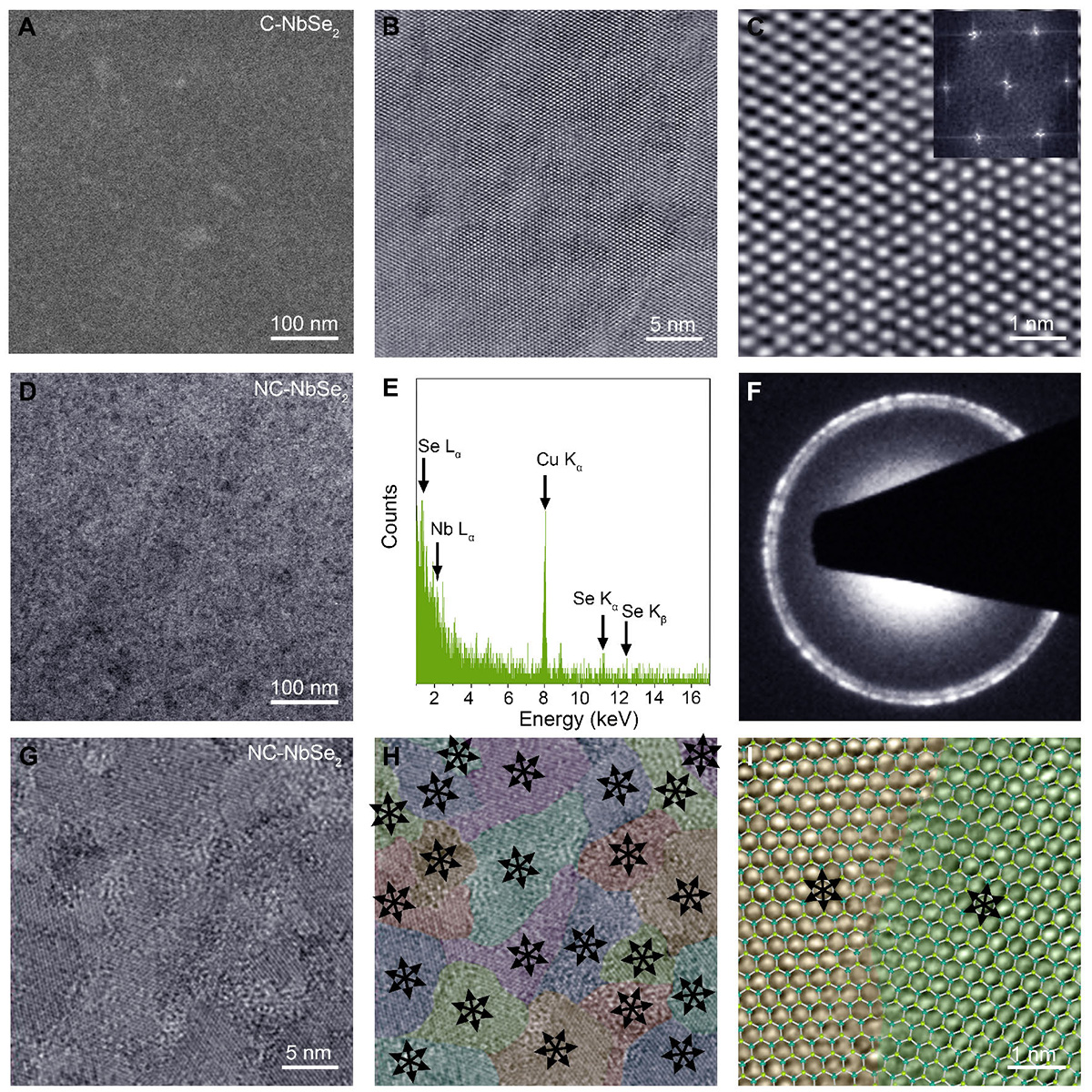
The nanocrystalline domains in NC-NbSe2 film. (A, B) Large-scale and (C) zoom-in high-resolution TEM images, and (inset in (C)) Fourier transform pattern of crystalline NbSe2 (C-NbSe2) film grown on a sapphire substrate as comparison. (D) A large-scale TEM image showing the uniformity of as-grown NC-NbSe2 film on SiO2/Si substrate. (E) The EDS spectrum and (F) SAED pattern of as-grown NC-NbSe2 film. Notably, the Cu Kα signal in panel (E) sources from the TEM grid. (G) A representative high-resolution TEM image with (H) false color and crystalline orientation superimposed to highlight nano-domain in NC-NbSe2 film. (I) A representative grain boundary between nano-domain in NC-NbSe2 film.
Current usage metrics show cumulative count of Article Views (full-text article views including HTML views, PDF and ePub downloads, according to the available data) and Abstracts Views on Vision4Press platform.
Data correspond to usage on the plateform after 2015. The current usage metrics is available 48-96 hours after online publication and is updated daily on week days.
Initial download of the metrics may take a while.