Figure 1
Download original image
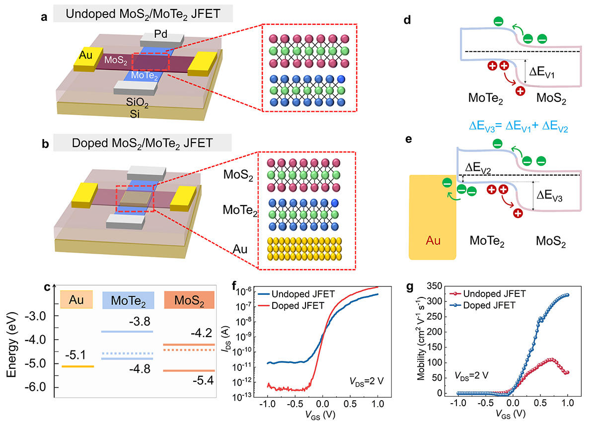
Comparisons of schematic diagrams, band structures and electrical properties between conventional and uniformly doped MoS2/MoTe2 JFET. (a, b) Schematic diagrams and atomic structures of the two JFETs. The red and green spheres represent MoS2, the blue and green spheres represent MoTe2, and the yellow spheres represent Au atoms. (c) The band diagrams of Au, MoTe2, and MoS2 before contact. (d, e) Band diagrams of the undoped (d) and Au-doped (e) MoS2/MoTe2 heterojunction. The ΔEV1 is the valence band offset when the MoS2/MoTe2 pn junction formed, which is about 0.6 eV. The ΔEV2 is the Schottky barrier height between Au and MoTe2, which is about 0.3 eV. The ΔEV3 is the valence band offset of the Au-doped MoS2/MoTe2 pn junction, while the ΔEV3 is approximately equal to ΔEV1 plus ΔEV2. (f) Transfer characteristics comparison with the VGS of 2 V. (g) The mobilities of undoped and doped JFETs with the VGS at 2 V.
Current usage metrics show cumulative count of Article Views (full-text article views including HTML views, PDF and ePub downloads, according to the available data) and Abstracts Views on Vision4Press platform.
Data correspond to usage on the plateform after 2015. The current usage metrics is available 48-96 hours after online publication and is updated daily on week days.
Initial download of the metrics may take a while.