| Issue |
Natl Sci Open
Volume 4, Number 5, 2025
|
|
|---|---|---|
| Article Number | 20250036 | |
| Number of page(s) | 9 | |
| Section | Materials Science | |
| DOI | https://doi.org/10.1360/nso/20250036 | |
| Published online | 03 September 2025 | |
RESEARCH ARTICLE
Electronic properties and quantum transport behavior of twisted γ-graphdiyne/graphene
1
Academy for Advanced Interdisciplinary Science and Technology, Key Laboratory of Advanced Materials and Devices for Post-Moore Chips, Ministry of Education, State Key Laboratory for Advanced Metals and Materials, University of Science and Technology Beijing, Beijing 100083, China
2
School of Materials Science and Engineering, Beijing Key Laboratory for Advanced Energy Materials and Technologies, University of Science and Technology Beijing, Beijing 100083, China
* Corresponding authors (emails: This email address is being protected from spambots. You need JavaScript enabled to view it.
(Zhuo Kang); This email address is being protected from spambots. You need JavaScript enabled to view it.
(Yue Zhang))
Received:
1
August
2025
Revised:
26
August
2025
Accepted:
29
August
2025
Abstract
Van der Waals heterostructures are acknowledged as a decent platform for electronic and optoelectronic applications owing to their atomically flat interfaces, unprecedented flexibility and unique physical characteristics. A twist angle between neighboring layers of two-dimensional materials renders with an additional mediator for flexible modulation of interlayer coupling and electrical structure. In this work, the carrier transport behavior of twisted moiré superlattices based on γ-graphdiyne, which is represented as the emerging category of carbon material family, is theoretically investigated for the first time. By probing a sequence of twisted γ-graphdiyne/graphene moiré superlattices, the sp-C is figured out to play a dominant role in manipulating the distribution of electron localization in the moiré system. The line and ring regions are identified as the primary geometric contributors to the density of states near the Fermi level in twisted γ-graphdiyne/graphene moiré superlattices. This twist engineering also enables to expedite quantum transport of γ-graphdiyne/graphene heterostructures according to the nonequilibrium Green’s function. This work unambiguously decodes the twist angle dependence of interlayer coupling for γ-graphdiyne/graphene heterobilayers and highlights the considerable enhancement of transport performance subtly triggered by a small twist angle (1°), benefiting a more in-depth understanding and rational design of emerging graphyne-based quantum devices.
Key words: γ-graphdiyne / moiré superlattice / transport behavior / transmission spectra
Contributed equally to this work.
© The Author(s) 2025. Published by Science Press and EDP Sciences.
 This is an Open Access article distributed under the terms of the Creative Commons Attribution License (https://creativecommons.org/licenses/by/4.0), which permits unrestricted use, distribution, and reproduction in any medium, provided the original work is properly cited.
INTRODUCTION
Moiré superlattices in heterostructures are formed when two layers of two-dimensional (2D) materials are vertically stacked with an interlayer twisting angle or lattice mismatch [1–3], which introduces an additional periodic potential energy landscape for in-plane carrier transport [4–7]. The twisted moiré superlattice provides a versatile and powerful platform for on-demand synthesis of artificial metamaterials [8–10]. In recent years, significant progress has been made in the study of many new quantum states in the moiré superlattice, such as unconventional superconductivity, correlated insulators, Hofstadter butterflies, and quantum criticality. In this regard, the twisting engineering creates fertile ground for independent manipulation of electronic band structure and charge density in these quantum material systems [11,12], which opens up a wide range of potential applications for bipolar device design such as light-emitting diodes, light diodes, and heterojunction bipolar transistors [13].
In many constructed graphene-based heterostructures, the weak van der Waals forces between the layers not only help to better preserve the respective electronic properties of each layer, but also give rise to a variety of novel physical properties [14]. γ-Graphdiyne (GDY) [15], an innovative sp/sp2-cohybridized carbon allotrope, has proven to be conducive to the design of multifunctional 2D materials and heterostructures by virtue of its high conjugation, abundant chemical bond activity and unique electronic properties [16–18]. The sp-hybridized carbon-carbon triple bond with many fascinating properties, especially the as-induced inhomogeneous distribution of surface charges, can trigger peculiar properties that other carbon materials do not possess [19–21]. It can be thus speculated that combining emerging GDY with classic graphene would make out interesting moiré superlattices featured with to-be-explored physicochemical properties, substantially enriching the content of twist engineering for more effective regulation of quantum transport behavior.
By means of Kohn-Sham density-functional theory (KS-DFT) [22], the interlayer twisting of GDY/graphene heterostructure is demonstrated to induce the formation of moiré patterns and reconstruction of the lattice structure along with an in-plane uneven interlayer coupling [23]. The distribution pattern of the interlayer electrostatic potential is further established in a series of twisted γ-GDY/graphene (TGG) moiré lattice models, revealing the ability of sp-C to dominate the local electron distribution in the moiré lattice system [24,25]. In addition, the density of states calculation suggests that the linear and ring regions are the main geometric factors apparently affecting the electronic properties for TGG moiré superlattices with different twisting angles. Further interpretation of the nonequilibrium Green’s function elucidates the effective facilitation effect of twist engineering on quantum transport in TGG moiré superlattices, and also reveals the significant enhancement of transport performance at a small twist angle (1°). These findings provide a solid theoretical foundation for a comprehensive understanding of this novel carbon material, shedding light on the design of high-performance quantum devices [26].
RESULTS AND DISCUSSION
We conducted first-principles calculations for the TGG moiré superlattice utilizing KS-DFT as implemented in the Vienna Ab initio Simulation Package (VASP), with twist angles ranging from 0° to 10°. The structural and electronic properties of the TGG at different twist angles were then examined (the specifics are presented in the METHODS section). The unit cell of the moiré superlattice, formed by a GDY/graphene bilayer, is shown in Figure 1. The TGG moiré superlattice is formed by rotating the GDY lattice with a slight angle θ relative to the other graphene lattice (as detailed in Section 1 of Supporting Information). Three distinct superlattices with angles θ = 0°, 1° and 10° were constructed, respectively (see the additional models in Section 3 of Supporting Information). Within all moiré superlattices, there are four local motifs that play crucial roles in determining the properties of the moiré lattices [27–29], labeled by AA, AB, Line and Ring. The domain AA with the highest energy is defined by the vertically oriented benzene ring located between the two layers due to spatial site resistance effects [30,31]. And the domain Ring is that the phenyl structure of graphene aligned perpendicular to the triangular pore structure of GDY with an energetically favorable stacking order. The atomic-scale reconstruction of stacking patterns is expected to enable manipulation of the electrical structure.
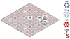 |
Figure 1 Structure of a TGG moiré superlattice with θ = 0°. Black lines indicate the cell boundary. The AA, AB, Ring and Line domains with high symmetry are framed. |
Due to the atomic rearrangement of the moiré superlattice, the obvious local interlayer coupling differences form a new moiré potential [26]. The local electrostatic potential on the TGG moiré superlattice is presented in Figure 2, which induces the potential fluctuation within the material. For θ values of 0°, 1°, and 10°, the interlayer electrostatic potential differences are measured to be 8, 38, and 23 meV, respectively. It is evident that the AA and AB regions are confined to the low potential area (colored red), whereas the Line and Ring regions are positioned within the high potential zone (colored blue). Additionally, a significant augmentation in the periodic electrostatic potential energy is observed following the twisting of the structures, which can be attributed to the fact that twisted dislocations promote pronounced changes in atomic arrangement and interlayer interactions in the different localized structural motifs [32]. The twist angle modulates charge localization strength by altering the aligned positions of sp-C in GDY and sp2-C in graphene, thereby altering the electrostatic potential distribution. Due to both synergistically contributing to the enhancement of the lattice potential, the Ring and Line regions are localized at the high potential region at θ = 1°, whereas the Line region is localized in the high potential area at θ = 10°. The sp-C motif of GDY generates a periodic electrostatic potential within the TGG moiré superlattice, which promotes the formation of charge localization and diverse electronic properties.
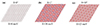 |
Figure 2 Electrostatic potential at three different angles of the TGG heterostructures. The blue isosurface indicates the high electrostatic potential region, and the red isosurface indicates the low electrostatic potential region. (a–c) Electrostatic potential in the GDY/graphene heterostructure with θ = 0°, 1°, 10°, respectively. |
The electronic properties of the TGG moiré superlattice are further investigated; the electronic structures and the charge densities of the conduction band minimum (CBM) and valence band maximum (VBM) states at various twist angles are calculated [33,34]. As for the band structure of the untwisted GDY/graphene heterostructure in Figure 3a, a direct band gap is evident with the valence band maximum and conduction band minimum situated at the K point in the TGG moiré superlattice. A 10 meV band gap opening is shown in the enlarged inset. The spatial distributions of the wave functions of CBM and VBM are illustrated in Figure 3b. The VBM and CBM charge density extends across both layers, with the primary contribution originating from the graphdiyne layer, leading to significant interlayer mixing. Moreover, the band gaps of the calculated band structures are observed to decrease upon twisting the structures, ranging from 3.4 meV in the heterostructure at θ = 1° to 6.1 meV in the heterostructure at θ = 10°, as presented in Figure 3c–f. The in-plane charge densities of the VBM and CBM reveal that the electron is more localized than the hole. The electron is subsequently trapped at the Line and Ring regions, which demonstrates that the sp-C of GDY is pivotal in charge localization. At a large twist angle of θ = 10°, the charge localization of the CBM is diminished. However, for a small angle of θ = 1°, the charge localization is much augmented. This can be attributed to the electrostatic potential inhomogeneities generated by the difference in the interlayer coupling, which modifies the potential periodicity and consequently disrupts the degeneracy of the π and π* bands at the K point, leading to the band gap opening as reported [35,36]. To further comprehend the origin of this band gap opening, the electrostatic potential difference was displayed (Figure S5).
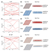 |
Figure 3 The electronic structure of the GDY/graphene heterostructures. (a) The band structure for the GDY/graphene heterostructure with θ = 0°. The CBM and VBM charge densities are shown in red and blue with the isosurface value establishing at 7 × 10⁻⁹ e Å−3, respectively. (b) Top and side views of the charge density of the CBM and VBM bands for the heterostructure with θ = 0°. The unit cell of the moiré lattice is indicated by the dashed box. (c) Band structure for the GDY/graphene heterostructure with θ = 1°. (d) Top and side views of the charge density of the CBM and VBM bands for the heterostructure with θ = 1°. (e) Band structure for the GDY/graphene heterostructure with θ = 10°. (f) Top and side views of the charge density of the CBM and VBM bands for the heterostructure with θ = 10°. |
To clarify the functional roles of different geometrical configurations in manipulating the electronic structure, specific contributions of the density of states (DOS) were dissected. The total DOS in Figure 4a with different angles show that the DOS of the system increases after twisting. Hence, it is a feasible route to effectively regulate the DOS via twisting. The DOS over various locations of the 0°, 1°, and 10° TGG moiré superlattice as shown in Figure 4b. It is evident that the density of states in the line and ring domains has been significantly increased within the TGG moiré superlattice. The sp-C motifs of GDY facilitate charge localization function [37], effectively regulating the position of the localized charge wave function.
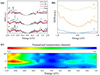 |
Figure 4 The transport property of the TGG moiré superlattice. (a) DOS of the TGG with θ = 0°, 1°, 10°. (b) Local density of states in the AA, AB, Line and Ring regions at different twist angles. (c) Carrier transmission spectra of the TGG moiré superlattice with different angles. |
To dive deep into the modulation effect of TGG moiré superlattice on electron transport behavior under different angles, we carried out an analysis of the electron transmission spectrum in Figure 4c, based on non-equilibrium Green’s function combined with density functional theory (NEGF-DFT) [38]. Owing to the non-uniform cross-sectional areas of individual devices, the transmission spectrum of each device was normalized by dividing by its respective cross-sectional area, yielding the “Normalized transmission”. We focus on presenting the spectral region around the Fermi level, as this segment makes the most significant contribution to carrier transport under low-bias conditions. For energies above the Fermi level, electron transmission is predominantly governed by the conduction bands of both materials. Notably, the electrons in GDY/graphene heterostructures with twist angles of 1° and 10° exhibit higher transmission coefficients and enhanced transport capabilities compared to those in the untwisted (θ = 0°) heterostructure. For energies below the Fermi level, transmission is predominantly governed by holes in the valence bands of both materials. Similarly, the holes in the 1° and 10° twisted heterostructures show greater transmission coefficients and improved transport performance relative to their counterparts in the θ = 0° system, indicating a more favorable hole transport configuration for device applications. This can be related to the enhancement of transmission, which is prompted by charge localization at the GDY/graphene contact. The modulation of electron and hole intensity is influenced by the twisted angle, which is advantageous for bipolar devices like light-emitting diodes, light diodes, and heterojunction bipolar transistors, allowing for adjustable carrier injection during manufacturing.
CONCLUSION
In summary, this work has effectively established the electronic properties and transport behavior of the TGG moiré superlattice at various twist angles by employing a state-of-the-art first-principles calculation. It is demonstrated that the interlayer distortion of the GDY/graphene heterostructure induces the formation of moiré patterns and lattice structure reconstruction with in-plane inhomogeneous interlayer coupling. The distribution pattern of the interlayer electrostatic potential is further established in a series of TGG moiré superlattice models. The charge localization induced by the sp-C motifs of GDY is theoretically clarified and demonstrated that the line and ring regions are the main geometrical configurations of the electronic properties in the TGG moiré superlattice. The modulation law of the electron transport behavior of the TGG moiré superlattice by twist engineering is deciphered, and the transmission spectrum demonstrates that the transmission window and intensity of the heterostructure can be effectively modulated by the twist angle to modify the transport behaviors. This work proposes a new scheme of twist engineering to control the transport properties and construct novel quantum devices, exploring new strategies for the creation of cutting-edge electronic and optoelectronic technologies.
METHODS
All calculation was carried out under the framework of density functional theory and non-equilibrium Green’s function [39]. The evaluation of carrier transport was simulated by a two-probe device with GDY and graphene as electrodes. We use projector augmented wave potential, while choose the generalized gradient approximation with the parametrization of Perdew-Burke-Ernzerhof to treat with the exchange correlation interaction. The cut-off energy of the plane-wave basis was set at 500 eV. The vacuum spacing in a direction perpendicular to the plane of the catalyst was set to at least 15 Å to prevent neighboring interaction Calculate the Hartree energy of the constructed model under different layer spacing models, and find the layer spacing corresponding to the minimum Hartree energy, that is, the layer spacing in an ideal case. Taking the 0° model as an example, the layer spacing of the two materials was set at 2.5 Å, and the self-consistent calculation was performed every 0.01 Å increase. Interface matching was controlled by strain the layered GDY in the searching for interfaces with mismatch as small as possible, making a trade-off between accuracy and computational resources. To be specific, the Chebyshev filtering technique is used, which has a high parallelization efficiency and prevents the enormous Kohn-Sham value issue from being diagonalized completely [40]. The precision of the computed results using such an approach is comparable to that of first-principles calculations using DFT, which has been supported by several previous studies [41–43].
Data availability
The original data are available from the corresponding authors upon reasonable request.
Acknowledgments
The authors thank Hongzhiwei Technology (Shanghai) Co. Ltd. for providing some computing technical support.
Funding
This work was supported by the National Key Research and Development Program of China (2022YFA1204502, 2021YFA1200196 and 2018YFA0703503), the National Natural Science Foundation of China (52122208, 52188101, 52072031, 51991340, 51991342 and 51702014), the Overseas Expertise Introduction Projects for Discipline Innovation (111 Project, B14003), the State Key Laboratory for Advanced Metals and Materials (2018Z-03 and 2019Z-04), and the Fundamental Research Funds for the Central Universities (QNXM20210013, FRF-TP-2021-03C1 and FRF-TP-20-008A3).
Author contributions
Y.L. and H.B. wrote the manuscript and analyzed the data. X.W. edited the manuscript. H.S., Z.X. and F.D. reviewed the formal analysis. Z.L. reviewed the manuscript. Z.K. and Y.Z. supervised the research.
Conflict of interest
The authors declare no conflict of interest.
Supplementary information
Supplementary file provided by the authors. Access Supplementary Material
References
- Cao Y, Fatemi V, Fang S, et al. Unconventional superconductivity in magic-angle graphene superlattices. Nature 2018; 556: 43-50. [Article] [NASA ADS] [CrossRef] [PubMed] [Google Scholar]
- Cao Y, Fatemi V, Demir A, et al. Correlated insulator behaviour at half-filling in magic-angle graphene superlattices. Nature 2018; 556: 80-84. [Article] [NASA ADS] [CrossRef] [PubMed] [Google Scholar]
- Chen G, Jiang L, Wu S, et al. Evidence of a gate-tunable Mott insulator in a trilayer graphene moiré superlattice. Nat Phys 2019; 15: 237-241. [Article] [Google Scholar]
- Shabani S, Halbertal D, Wu W, et al. Deep moiré potentials in twisted transition metal dichalcogenide bilayers. Nat Phys 2021; 17: 720-725. [Article] [Google Scholar]
- Tang K, Qi W. Moiré-pattern-tuned electronic structures of van der Waals heterostructures. Adv Funct Mater 2020; 30: 2002672. [Article] [Google Scholar]
- Yoo H, Engelke R, Carr S, et al. Atomic and electronic reconstruction at the van der Waals interface in twisted bilayer graphene. Nat Mater 2019; 18: 448-453. [Article] [Google Scholar]
- Zhao P, Xiao C, Yao W. Universal superlattice potential for 2D materials from twisted interface inside h-BN substrate. npj 2D Mater Appl 2021; 5: 38. [Article] [Google Scholar]
- Shimazaki Y, Schwartz I, Watanabe K, et al. Strongly correlated electrons and hybrid excitons in a moiré heterostructure. Nature 2020; 580: 472-477. [Article] [Google Scholar]
- Tang Y, Li L, Li T, et al. Simulation of Hubbard model physics in WSe2/WS2 moiré superlattices. Nature 2020; 579: 353-358. [Article] [CrossRef] [PubMed] [Google Scholar]
- Lau CN, Bockrath MW, Mak KF, et al. Reproducibility in the fabrication and physics of moiré materials. Nature 2022; 602: 41-50. [Article] [Google Scholar]
- Yankowitz M, Chen S, Polshyn H, et al. Tuning superconductivity in twisted bilayer graphene. Science 2019; 363: 1059-1064. [Article] [Google Scholar]
- Brzhezinskaya M, Kononenko O, Matveev V, et al. Engineering of numerous moiré superlattices in twisted multilayer graphene for twistronics and straintronics applications. ACS Nano 2021; 15: 12358-12366. [Article] [Google Scholar]
- Zhu J, Shang W, Ning J, et al. Twisted angle modulated structural property, electronic structure and carrier transport of MoS2/AlN(0001) mixed-dimensional van der Waals heterostructure. Appl Surf Sci 2021; 563: 150330. [Article] [Google Scholar]
- Wang L, Zihlmann S, Liu MH, et al. New generation of moiré superlattices in doubly aligned hBN/graphene/hBN heterostructures. Nano Lett 2019; 19: 2371-2376. [Article] [Google Scholar]
- Fang Y, Liu Y, Qi L, et al. 2D graphdiyne: An emerging carbon material. Chem Soc Rev 2022; 51: 2681-2709. [Article] [Google Scholar]
- Yan H, Yu P, Han G, et al. High-yield and damage-free exfoliation of layered graphdiyne in aqueous phase. Angew Chem Int Ed 2019; 58: 746-750. [Article] [Google Scholar]
- Li Y, Xu L, Liu H, et al. Graphdiyne and graphyne: From theoretical predictions to practical construction. Chem Soc Rev 2014; 43: 2572-2586. [Article] [Google Scholar]
- Hu G, He J, Chen J, et al. Self-assembly of wheel-shaped nanographdiynes and self-template growth of graphdiyne. J Am Chem Soc 2024; 146: 4123-4133. [Article] [Google Scholar]
- Liu Y, Dai F, Bai H, et al. Exciton localization modulated by ultradeep moiré potential in twisted bilayer γ-graphdiyne. J Am Chem Soc 2024; 146: 14593-14599. [Article] [Google Scholar]
- Ma K, Wu J, Wang X, et al. Periodically Interrupting Bonding Behavior to Reformat Delocalized Electronic States of Graphdiyne for Improved Electrocatalytic Hydrogen Evolution. Angew Chem Int Ed 2022; 61: e202211094. [Article] [Google Scholar]
- Fan W, Zhang S, Xu C, et al. Grain boundary perfection enabled by pyridinic nitrogen doped graphdiyne in hybrid perovskite. Adv Funct Mater 2021; 31: 2104633. [Article] [Google Scholar]
- Michaud-Rioux V, Zhang L, Guo H. RESCU: A real space electronic structure method. J Comput Phys 2016; 307: 593-613. [Article] [Google Scholar]
- Xiao Y, Liu J, Fu L. Moiré is more: Access to new properties of two-dimensional layered materials. Matter 2020; 3: 1142-1161. [Article] [Google Scholar]
- Brandbyge M, Mozos JL, Ordejón P, et al. Density-functional method for nonequilibrium electron transport. Phys Rev B 2002; 65: 165401. [Article] [Google Scholar]
- Smidstrup S, Stradi D, Wellendorff J, et al. First-principles Green’s-function method for surface calculations: A pseudopotential localized basis set approach. Phys Rev B 2017; 96: 195309. [Article] [Google Scholar]
- Song JCW, Gabor NM. Electron quantum metamaterials in van der Waals heterostructures. Nat Nanotech 2018; 13: 986-993. [Article] [Google Scholar]
- Tran K, Moody G, Wu F, et al. Evidence for moiré excitons in van der Waals heterostructures. Nature 2019; 567: 71-75. [Article] [NASA ADS] [CrossRef] [PubMed] [Google Scholar]
- Yuan L, Zheng B, Kunstmann J, et al. Twist-angle-dependent interlayer exciton diffusion in WS2-WSe2 heterobilayers. Nat Mater 2020; 19: 617-623. [Article] [Google Scholar]
- Tartakovskii A. moiré or not. Nat Mater 2020; 19: 581-582. [Article] [Google Scholar]
- Weston A, Zou Y, Enaldiev V, et al. Atomic reconstruction in twisted bilayers of transition metal dichalcogenides. Nat Nanotechnol 2020; 15: 592-597. [Article] [Google Scholar]
- Zhang S, Xu Q, Hou Y, et al. Domino-like stacking order switching in twisted monolayer-multilayer graphene. Nat Mater 2022; 21: 621-626. [Article] [Google Scholar]
- Tao S, Zhang X, Zhu J, et al. Designing ultra-flat bands in twisted bilayer materials at large twist angles: theory and application to two-dimensional indium selenide. J Am Chem Soc 2022; 144: 3949-3956. [Article] [Google Scholar]
- Guo H, Zhang X, Lu G. Shedding light on moiré excitons: A first-principles perspective. Sci Adv 2020; 6: eabc5638. [Article] [Google Scholar]
- Wang H, Ma S, Zhang S, et al. Intrinsic superflat bands in general twisted bilayer systems. Light Sci Appl 2022; 11: 159. [Article] [Google Scholar]
- Xiao Z, Shupeng S, Huiqi L, et al. First principles study on the electronic structure and optical properties of graphene/MoS2 heterojunctions with different rotation angles. Chin J High Press Phys 2024; 38: 052201 [Google Scholar]
- Kim S, Ihm J, Choi HJ, et al. Origin of anomalous electronic structures of epitaxial graphene on silicon carbide. Phys Rev Lett 2008; 100: 176802. [Article] [Google Scholar]
- Kang J, Li J, Wu F, et al. Elastic, electronic, and optical properties of two-dimensional graphyne sheet. J Phys Chem C 2011; 115: 20466-20470. [Article] [Google Scholar]
- Naserian S, Izadyar M, Ranjbakhsh E. Theoretical design of Au–DPPh–Au molecular junction for use in organic field-effect transistors. J Phys Chem Solids 2023; 180: 111440. [Article] [Google Scholar]
- Smidstrup S, Markussen T, Vancraeyveld P, et al. QuantumATK: An integrated platform of electronic and atomic-scale modelling tools. J Phys-Condens Matter 2019; 32: 015901. [Article] [Google Scholar]
- Zhou Y, Saad Y, Tiago ML, et al. Parallel self-consistent-field calculations via Chebyshev-filtered subspace acceleration. Phys Rev E 2006; 74: 066704. [Article] [Google Scholar]
- Liu D, Chen X, Hu Y, et al. Raman enhancement on ultra-clean graphene quantum dots produced by quasi-equilibrium plasma-enhanced chemical vapor deposition. Nat Commun 2018; 9: 193. [Article] [Google Scholar]
- Lin W, Li J, Wang W, et al. Electronic structure and band gap engineering of two-dimensional octagon-nitrogene. Sci Rep 2018; 8: 1674. [Article] [Google Scholar]
- Hu C, Michaud-Rioux V, Kong X, et al. Dirac electrons in moiré superlattice: From two to three dimensions. Phys Rev Mater 2017; 1: 061003. [Article] [Google Scholar]
All Figures
|
Figure 1 Structure of a TGG moiré superlattice with θ = 0°. Black lines indicate the cell boundary. The AA, AB, Ring and Line domains with high symmetry are framed. |
| In the text | |
|
Figure 2 Electrostatic potential at three different angles of the TGG heterostructures. The blue isosurface indicates the high electrostatic potential region, and the red isosurface indicates the low electrostatic potential region. (a–c) Electrostatic potential in the GDY/graphene heterostructure with θ = 0°, 1°, 10°, respectively. |
| In the text | |
|
Figure 3 The electronic structure of the GDY/graphene heterostructures. (a) The band structure for the GDY/graphene heterostructure with θ = 0°. The CBM and VBM charge densities are shown in red and blue with the isosurface value establishing at 7 × 10⁻⁹ e Å−3, respectively. (b) Top and side views of the charge density of the CBM and VBM bands for the heterostructure with θ = 0°. The unit cell of the moiré lattice is indicated by the dashed box. (c) Band structure for the GDY/graphene heterostructure with θ = 1°. (d) Top and side views of the charge density of the CBM and VBM bands for the heterostructure with θ = 1°. (e) Band structure for the GDY/graphene heterostructure with θ = 10°. (f) Top and side views of the charge density of the CBM and VBM bands for the heterostructure with θ = 10°. |
| In the text | |
|
Figure 4 The transport property of the TGG moiré superlattice. (a) DOS of the TGG with θ = 0°, 1°, 10°. (b) Local density of states in the AA, AB, Line and Ring regions at different twist angles. (c) Carrier transmission spectra of the TGG moiré superlattice with different angles. |
| In the text | |
Current usage metrics show cumulative count of Article Views (full-text article views including HTML views, PDF and ePub downloads, according to the available data) and Abstracts Views on Vision4Press platform.
Data correspond to usage on the plateform after 2015. The current usage metrics is available 48-96 hours after online publication and is updated daily on week days.
Initial download of the metrics may take a while.