| Issue |
Natl Sci Open
Volume 4, Number 5, 2025
|
|
|---|---|---|
| Article Number | 20250034 | |
| Number of page(s) | 12 | |
| Section | Materials Science | |
| DOI | https://doi.org/10.1360/nso/20250034 | |
| Published online | 20 August 2025 | |
RESEARCH ARTICLE
Uniform doping for MoS2/MoTe2 van der Waals junction field-effect transistors with ideal subthreshold slope
1
Academy for Advanced Interdisciplinary Science and Technology, Key Laboratory of Advanced Materials and Devices for Post-Moore Chips, Ministry of Education, State Key Laboratory for Advanced Metals and Materials, University of Science and Technology Beijing, Beijing 100083, China
2
Future Chip Materials & Technology Innovation Center, School of Future Technology, School of Materials Science and Engineering, Beijing Key Laboratory for Advanced Energy Materials and Technologies, University of Science and Technology Beijing, Beijing 100083, China
* Corresponding authors (emails: This email address is being protected from spambots. You need JavaScript enabled to view it.
(Zheng Zhang); This email address is being protected from spambots. You need JavaScript enabled to view it.
(Xiankun Zhang); This email address is being protected from spambots. You need JavaScript enabled to view it.
(Yue Zhang))
Received:
26
July
2025
Revised:
17
August
2025
Accepted:
19
August
2025
Abstract
Two-dimensional (2D) semiconductor-based junction field-effect transistors (JFETs) have emerged as vital architectures for next-generation low-power electronics due to their gate-dielectric-free structure and near-ideal subthreshold swing (SS) potential. Although doping strategies, such as defect engineering and chemical modification, can further enhance the performance of JFETs, complex techniques and uniformly-doping hinder their further applications. Here, we propose a low-power MoS2/MoTe2 JFET utilizing a pre-deposited Au film to dope the gate layer of MoTe2, which can uniformly increase the work function of MoTe2 and thus elevate heterostructure barrier heights. This method offers strong repeatability, avoids localized states on channel material, and is compatible with integrated circuit manufacturing. The JFETs achieve a near-ideal SS of 62.5 mV dec−1, mobility of 350 cm2 V−1 s−1, high current on/off ratio of 107, low gate leakage of 10−12 A, and low pinch-off voltage of −0.1 V. This strategy provides a universal and simple strategy for low-power circuits.
Key words: junction field-effect transistor / two-dimensional materials / MoS2/MoTe2 heterojunction / electrostatic doping / subthreshold swing / low-power electronics
Contributed equally to this work.
© The Author(s) 2025. Published by Science Press and EDP Sciences.
 This is an Open Access article distributed under the terms of the Creative Commons Attribution License (https://creativecommons.org/licenses/by/4.0), which permits unrestricted use, distribution, and reproduction in any medium, provided the original work is properly cited.
INTRODUCTION
As the most widely used transistor at present, silicon-based metal-oxide-semiconductor field-effect transistor (MOSFET) has been constrained by the evolution of Moore’s Law, the whole size continues to shrink and is approaching the physical limit, resulting in a sharp increase in power consumption [1–6]. Junction field-effect transistor (JFET) without the dielectric layer has become one of the effective alternative solutions to MOSFET, which can perfectly avoid strong phonon scattering between the channel material and the dielectric layer [7–10]. By adjusting the depletion layer width formed by the heterojunction, the channel current is controlled to achieve ON and OFF states. More importantly, the subthreshold swing (SS) for MOSFET is defined as [11]
while
where IDS and VGS represent the source-drain current and the gate-source voltage of the transistor, respectively. Due to the dielectric-free configuration and the higher doping concentration of the gate compared to the channel, the JFET behaves similar to a MOSFET with a very large gate capacitance. Since the capacitance from the source to the channel is much smaller than that from the gate to the channel, the SS of JFET can approach the Boltzmann limit of 60 mV dec−1 easily [8]. Unlike silicon-based transistors, two-dimensional (2D) transition metal dichalcogenides (TMDCs) have become attractive channel materials for constructing low-power electronics due to their atom-scale thickness, dangling-bond-free surface, tunable bandgap, and high carrier mobility [12–14]. However, there are still certain technical challenges in achieving a 2D JFET that simultaneously possesses high mobility, high on-off ratio, and ultra-low SS due to the limited heterojunction depletion region and barrier height [15–18]. Lim et al. [19] reported a MoTe2/MoS2 van der Waals (vdWs) JFET and realized a near-zero threshold voltage. However, the performance of the p-channel is far inferior to that of the n-channel, leading to a small gate adjustment capability. An appropriate doping strategy can effectively increase the carrier concentration and enhance the performance of the JFETs [20]. The standard doping methods include chemical doping and molecular doping [21]. Chemical doping is mainly achieved by adding dopants to the material surface. Since dopants are inherently dispersed in the form of particles, localized non-uniform doping is inevitable [22]. Such non-uniformity introduces local fields, leading to uneven regulation of barrier height and, consequently, a tendency to induce leakage current. Molecular doping is also called absorbate-induced doping that depends on the surface charge transfer of organic molecular materials to a semiconductor [9,23,24]. Compared with the chemical doping method, molecular doping also encounters difficulties in removing organic molecules and instability in doping. Therefore, there is an urgent need to develop a stable and uniform doping control method to obtain high-performance and low-power transistors.
Here, we fabricated a uniformly Au-doped MoS2/MoTe2 van der Waals JFET, and MoTe2 is used as the gate while MoS2 serves as the n-channel. Compared with the undoped MoS2/MoTe2 JFET (Figure 1a), the MoTe2 needs to be transferred onto the pre-deposited Au completely to obtain uniformly electrostatic doping (Figure 1b). The band diagram in Figure 1c indicated that the work function of Au is 5.1 eV, the bottom of the conduction band and the top of the valence band of MoTe2 (MoS2) are about −3.8 eV (−4.2 eV) and −4.8 eV (−5.4 eV) [25–27]. The band diagram of the MoTe2 and MoS2 after contact is displayed in Figure 1d. When the two materials come into contact, the minority carrier holes in MoTe2 are injected into MoS2, while the minority carrier electrons in MoS2 are injected into MoTe2. Eventually, the movement of carriers reaches an equilibrium state, and the valence band offset of the MoS2/MoTe2 heterojunction is about 0.6 eV (ΔEV1). The Schottky barrier height between Au and MoTe2 refers to the difference in work function of Au to the electron affinity of MoTe2, which is about 0.3 eV (ΔEV2). The bottom Au-doping effect will bring the Fermi level of MoTe2 closer to the valence band without inducing the additional local state, thereby increasing the barrier height (ΔEV3) of the MoS2/MoTe2 heterojunction, and the ΔEV3 is approximately equal to ΔEV1 plus ΔEV2 (Figure 1e). Thus, the n-type JFETs can achieve effective pinch-off for the MoS2 channel, exhibiting an obviously enhanced current on-off ratio and enlarged the mobility compared to the undoped MoS2/MoTe2 JFET (Figure 1f, g).
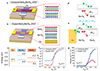 |
Figure 1 Comparisons of schematic diagrams, band structures and electrical properties between conventional and uniformly doped MoS2/MoTe2 JFET. (a, b) Schematic diagrams and atomic structures of the two JFETs. The red and green spheres represent MoS2, the blue and green spheres represent MoTe2, and the yellow spheres represent Au atoms. (c) The band diagrams of Au, MoTe2, and MoS2 before contact. (d, e) Band diagrams of the undoped (d) and Au-doped (e) MoS2/MoTe2 heterojunction. The ΔEV1 is the valence band offset when the MoS2/MoTe2 pn junction formed, which is about 0.6 eV. The ΔEV2 is the Schottky barrier height between Au and MoTe2, which is about 0.3 eV. The ΔEV3 is the valence band offset of the Au-doped MoS2/MoTe2 pn junction, while the ΔEV3 is approximately equal to ΔEV1 plus ΔEV2. (f) Transfer characteristics comparison with the VGS of 2 V. (g) The mobilities of undoped and doped JFETs with the VGS at 2 V. |
MATERIALS AND METHODS
Fabrication of Au-doped and undoped MoS2/MoTe2 vdWs JFETs
Mechanical exfoliation was used to obtain few-layer MoS2 and MoTe2. The bulk MoS2 and MoTe2 were purchased from 6 Carbon Technology (Shenzhen). The vdWs MoS2/MoTe2 heterostructure was built using a precise transfer platform (Metatest, E1-T) with the dry-accurate transfer method. First, a 10 nm-thick Au film is deposited on the substrate. Subsequently, MoS2 and MoTe2 flakes with thicknesses of approximately 4 and 8 nm, respectively, are obtained via mechanical exfoliation. Next, the MoTe2 flake is transferred onto the Au film surface using a precision transfer platform. Following this, the MoS2 flake is stacked onto the MoTe2 surface in a perpendicularly crossed orientation. During this step, it is essential to ensure that the selected MoTe2 flake exhibits a uniform size comparable to that of the bottom electrode (Au film) and fully covers it to prevent direct contact between MoS2 and the bottom electrode, which would cause short-circuit failure of the device. The precise transfer technology enables a super-clean interface of the vdWs integrated MoS2/MoTe2 heterojunction. Finally, the electrode pattern was formed by electron beam exposure, and contact metals were deposited via a high-vacuum electron-beam evaporation system (KYKY). A 10/50 nm Pd/Au electrode is deposited on the MoTe2 surface, while a 60 nm-thick Au electrode is deposited on the MoS2 surface.
Characterization
Optical microscopy was used to determine the morphology of MoS2 and MoTe2 crystals (Olympus BX-51M). Kelvin probe force microscope (KPFM) and atomic force microscope (AFM) images were measured under the AFM (Bruker dimension ICON). A Pt/Ir-coated conductive tip (SCM-PIT-V2, Bruker Nano Inc.,) was chosen to probe the morphology and thickness of MoS2 and MoTe2 under the ScanAsyst mode, while AM-KPFM measurement was performed in the tapping mode using the same model tip with a resonant frequency of 75 kHz and a tip radius of 25 nm. Raman spectrum was performed under the confocal microscope (JY-HR800) at room temperature with a power of 20 mW and a 532 nm laser. The laser spot size was about 1 mm2. The electrical properties were realized by the semiconductor analysis system (Keithley 4200).
RESULTS AND DISCUSSION
To investigate the influence of uniform doping on MoTe2, we conducted a comparative experiment on the performance of MoTe2 field-effect transistors (FETs) doped with Au and without Au (Figure 2a). The fabrication process can be found in the Section MATERIALS AND METHODS. To enhance the device performance of Au-doped MoS2/MoTe2 heterojunctions, it is critical to minimize the non-overlapping regions of Au, MoS2, and MoTe2 in the JFET, which inherently complicates AFM height measurements. Therefore, we roughly estimate the thicknesses of MoS2 and MoTe2 based on their colors. A series of samples was selected based on their characteristic colors, and their corresponding thicknesses were measured (Figure S1). Subsequently, during device fabrication, materials with specific colors were consistently chosen to ensure controlled thicknesses. To ensure the optimal contact of MoTe2 with metal, we fabricated three MoTe2 FETs with 10 nm/50 nm-thick Cr/Au, 60 nm-thick Au and 10 nm/50 nm-thick Pd/Au electrodes, respectively (Figures S2–S4). The output characteristics of all three devices showed good ohmic contact but exhibited distinct charge transport behavior. The MoTe2 FET with Cr/Au contact exhibited electron-dominated transport (Figure S2), while the MoTe2 FET with Au contact showed a symmetrical bipolar behavior (Figure S3). In contrast, the MoTe2 FET with Pd/Au contact exhibited hole-dominated transport behavior, characterized by a positive shift in the gate voltage turn-on point and enhanced hole concentrations (Figure S4). The higher metal work function of Pd made the metal Fermi level closer to the valence band edge of MoTe2, which reduced the hole injection barrier and promoted hole transport. Therefore, the Pd/Au electrodes are selected to fabricate MoTe2 FETs to achieve good hole-dominated transport behavior in the following devices. The transfer characteristics of the Pd/Au contacted MoTe2 FETs in Figure 2b show prominent p-type transfer characteristics of both uniform doped and undoped MoTe2 FETs. Still, the inflection point of the transfer curve of the uniformly Au-doped MoTe2 FET is located at a more positive gate voltage, proving the hole concentration is significantly higher than that of the undoped MoTe2 FET. Although the Au film did not completely cover the entire layer of MoTe2, the output characteristics of the MoTe2 FETs in Figure S5 exhibited good ohmic contacts in both undoped and Au-doped MoTe2, indicating that the doping of the MoTe2 channel was relatively uniform. This may be because although Au doping can achieve local charge injection into MoTe2, the carriers migrate toward the source and drain electrodes simultaneously, eventually making the electrical transport of the transistor exhibit ohmic contact. To further determine the doping effect, Raman characterization of MoTe2 on SiO2 and on Au film was performed, equipped with the 532 nm wavelength laser, respectively, as shown in Figure 2c. The 186 and 231 cm−1 in the spectra of 2H-MoTe2 correspond to the A1g and  mode, respectively [28]. Additionally, the difference of the A1g peak is enlarged for analysis. Compared with MoTe2 on SiO2, Raman spectra of MoTe2 on Au exhibit an evident blue shift by 1 cm−1, while the shift of
  peak cannot be observed obviously. In MoTe2 characteristic Raman peaks, the
  represents the in-plane vibrational mode, while the A1g represents the out-of-plane vibration mode. The
  mode is quite sensitive to uniaxial strains, while the strain effect cannot affect the A1g mode [29,30]. On the other hand, doping can change the A1g mode of vibration but has no impact on the
  vibrational mode. According to the blueshift of the A1g peak in Figure 2c, it can be proved that Au indeed has a hole-doped effect on MoTe2. In addition, we also used the KPFM to characterize the potential difference of MoTe2 contacted with and without Au. Contact potential difference (CPD) usually indicates the difference in work function between the sample and AFM tip [31]. Significant changes in the surface potential between Au-doped MoTe2 and undoped MoTe2 are distinguished (Figure 2d). The potential line profile across the heterostructure edge corresponds to the white line in Figure 2d, implying a Fermi level difference of 40 mV, indicating that the Fermi level of MoTe2 lying on the Au film moves downward. As shown in Figure 2f, the energy bands of the undoped and the Au-doped MoTe2/MoS2 heterojunction indicate that the barrier height of the latter one is higher, which can greatly enhance the depletion region of the heterojunction.
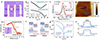 |
Figure 2 Multi-angle comparisons of uniformly Au-doped and undoped MoTe2 FETs. (a) Optical image of the two MoTe2 FETs. (b) Drain voltage dependent transfer characteristic curves. (c) Raman curves of uniformly doped and undoped MoTe2. (d) Surface potential image of MoTe2 on Au and SiO2 substrates. (e) Potential line profile across the edge of the Au corresponding to the white line in (d). The inset is the optical microscope image of MoTe2 layer stack on the Au film and the insulating silicon substrate. (f) Band alignment of MoTe2/MoS2 heterojunction with the undoped MoTe2 (left) and the doped MoTe2 (right). (g) Rectification curves of doped and undoped MoS2/MoTe2 pn junction. (h) Band diagrams of the uniformly doped (blue) and undoped (grey) MoS2 along the channel length. |
Furthermore, the diode characteristics of the gate-channel heterojunction are essential in determining the eventual performance of the JFETs. The rectification characteristics of the pn junction are systematically measured, as shown in Figure 2g. It was found that the rectification ratio (RR) of the doped JFET can be achieved at 104, which is significantly higher than that of the undoped JFET of 2×10². Similar results are also obtained for the output characteristics, as shown in Figures S6 and S7. It is further proved that the uniformly doped heterojunction has good rectification characteristics, laying a foundation for the subsequent excellent device performance. The band structure of uniformly doped (blue) and undoped (gray) MoS2 is also drawn in Figure 2h. Under the same gate voltage, the energy band of doped MoS2 is more bent up than that of the undoped MoS2, which can be easily depleted.
As mentioned above, theoretically, JFET is superior to MOSFET in the sub-threshold region due to its dielectric-free device structure. Figure 3a is an optical microscope image of a uniformly doped MoS2/MoTe2 JFET. The electrical properties of the JFET under different gate voltages were measured, as shown in Figure 3b. At zero gate voltage, the output characteristic curve is easily saturated. As the gate voltage gradually increases, the saturation speed of the output characteristic curve gradually slows down. Based on the output characteristic curves of the JFET, they can be divided into the linear region, pinch-off region, and saturation region. In the linear region, the source-drain voltage of VDS is small, the longitudinal electric field dominates the channel. The electric field intensity in the channel is low and uniformly distributed. The mobility is close to the intrinsic mobility of the material. At this point, carrier scattering is mainly determined by lattice vibrations and impurity scattering, and is only weakly affected by the electric field intensity, so the mobility approximates a constant. In the pinch-off region, as VDS increases, the electric field intensity on the side of the channel close to the drain electrode increases significantly, leading to pinch-off of the channel in this region. As a result, the carrier drift velocity begins to deviate from the linear relationship, and the mobility decreases noticeably with the increase of electric field intensity. In the saturation region, the pinch-off region of the channel expands toward the source, and the average electric field intensity of the entire channel further increases. At this time, the drain current IDS no longer changes significantly with VDS, and the carrier drift velocity approaches the saturation velocity. Here, with the increase of electric field intensity, the mobility exhibits an approximately inverse proportional decay and tends to stabilize [8]. Figure 3c, d shows the typical transfer characteristics of MoS2/MoTe2 JFET under different source-drain voltages by a logarithmic diagram and a linear diagram, respectively. As shown in Figure 3c, the n-type transport behavior of the JFET was obtained with a switching ratio of about 107. The SS can be expressed as the reciprocal of the slope of the subthreshold region of the transfer characteristic, where 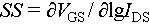 . The smaller the SS value, the stronger the gate voltage’s ability to regulate the channel current [32]. Notably, the IDS-VGS slope in the subthreshold region is about 62.5 mV dec−1, close to the theoretical limit. Additionally, gate leakage current measurements of the doped JFET revealed values of about 10−12 A, which reveals that uniform doping not only significantly decreased the SS, but also substantially reduced the gate leakage current. The pinch-off voltage (Vp) refers to the critical voltage at which the channel is completely depleted when the VGS reaches a specific value, causing the IDS approach to zero. During measurement, the VDS needs to be kept constant. When IDS decreases to below 1 pA as VGS changes, the corresponding VGS is the Vp [8,32]. As shown in Figure 3d, the pinch-off voltage of Vp is only −0.1 V through the intersection of the linear partial reverse extension line and the transverse gate voltage. To quantitatively study the performance of MoS2/MoTe2 JFET in the subthreshold region, SS and IDS are plotted as the gate voltage functions (Figure 3e). It is obvious that the values of SS are close to the ideal value of 60 mV dec−1. The transconductance (gm) is a parameter that represents the current gain influenced by the gate voltage, which is calculated by Eq. (1) and shown in Figure 3f. The maximum transconductance of the Au-doped MoS2/MoTe2 JFET can reach 7.68 μS at VDS=1 V.
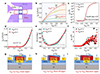 |
Figure 3 Electrical properties of Au-doped MoS2/MoTe2 JFET with MoS2 serves as channel material and MoTe2 serves as gate materials. (a) Optical microscope image of the MoS2/MoTe2 JFET. (b) Output characteristic curves of the MoS2/MoTe2 JFET. The three working stages represent (i) linear region, (ii) pinch-off region, and (iii) saturation region. (c) Drain voltage dependent transfer characteristic curves. (d) Linear plot of the transfer characteristic curves. The pinch-off voltage VP of the JFET is −0.10 V. (e) The SS extracted at different VDS at room temperature. (f) The gm as a function of gate voltage at the VDS of 1 and 2 V. (g–i) Cross-sectional view of the depletion region of the JFET at three stages of (g) linear region, (h) pinch-off region, and (i) saturation region, corresponding to the output characteristics in (b). The d represents the distance between the edge of the Au and MoS2 in the JFET. |
 (1)
(1)
The mobility of the JFET is defined as the average drift velocity of carriers under a unit electric field. Specifically, it refers to the movement efficiency of carriers in the channel region under the combined action of the transverse electric field formed by the gate voltage and the longitudinal electric field formed by the source-drain voltage. Here, the maximum mobility of JFET is extracted utilizing the following calculation formula when the JFET is in the saturation region and the transconductance reaches the maximum value [33]:
 (2)
(2)
where Nd is the number of carrier concentrations of charges per cubic centimeter, which is estimated by the Hall measurement. q is the electronic charge. t, W, and L are the thickness, width, and length of the channel, respectively. Nd can be estimated through the Hall effect by measuring the electron carrier density at zero gate voltage, which is estimated as 2.5×1016 cm−3 at 300 K. Ultimately, the mobility curve of this device is attained, and the peak value of the mobility achieves 350 cm2 V−1 s−1, which is similar to the typical MoS2 MOSFET.
To obtain a comprehensive understanding of the working mechanism of the Au-doped MoS2/MoTe2 JFETs, the schematic diagrams of the junction depletion region driven by both VGS and VDS are shown in Figure 3g–i. As mentioned above, to improve the performance of Au-doped MoS2/MoTe2 heterojunction devices, it is essential to reduce the non-overlapping areas of Au, MoS2, and MoTe2 as much as possible. Therefore, the distance (d) between the edge of the Au film and MoS2 layer in Figure 3g should be as small as possible. At the same time, the Au film must not come into contact with MoS2 to prevent short circuits. Similar to MOSFET, JFET has an asymmetric depletion region. When the device operates in the linear region corresponding to Figure 3b(i), due to the small depletion region, the carrier in MoS2 can inject from the source electrode to the drain electrode fluently. Because of the presence of a voltage gradient in the channel, the source voltage is higher than the drain voltage, which results in a lower barrier. The junction potential near the drain is lower, thereby tilting the depletion region toward the drain (Figure 3g). This effect becomes more pronounced as VDS increases up the VGS−VP due to the change in the electric field strength distribution in the channel, as shown in Figure 3h. When VGS−VP=VDS, the channel is completely shut down, and the device operates in the pinch-off region corresponding the Figure 3b(ii). As the VDS continues to increase, and then VGS−VP<VDS, the pinch-off region extends further, as shown in Figure 3i. The inclined depletion region causes the JFET to reach the saturation region state, and the device exhibits stable IDS with the increase of VDS [16,34]. Compared with the undoped-MoS2/MoTe2 JFET, the underlying Au film will increase the work function of MoTe2, making its Fermi level closer to the valence band. As a result, the barrier height between MoTe2 and MoS2 will be increased, and therefore, accelerating the depletion rate of the MoS2 channel.
To intuitively present the advantages of the doping effect, the electrical properties of the undoped MoS2/MoTe2 JFET are tested. The thicknesses of MoS2 and MoTe2 used are consistent with that of the uniform doped devices with a MoTe2 of 8 nm (Figure S8). The obtained output characteristics are shown in Figure 4a, and also have three typical working stages of linear region, pitch-off region, and saturation region. Figure 4b, c also shows the transfer characteristic curves of the logarithmic and linear relationship of the VGS-IDS. According to Figure 4b, the current on-off ratio and SS are about 105 and 113 mV dec−1, respectively. By extracting the linear part, the pinch-off voltage of Vp is about −0.18 V. Similarly, the values of SS curves under different bias voltages are about 100 mV dec−1 in Figure 4d, which is far from the ideal subthreshold. Finally, the saturated mobility of undoped MoS2/MoTe2 JFET is calculated, and the peak mobility is about 130 cm2 V−1 s−1 (Figure 4e). Due to the dangling-free surface of the 2D vdWs heterojunction, the interface capture state of the JFET caused by defects can be minimized. However, due to the bipolar nature of MoTe2, the barrier height formed with MoS2 is not high enough to allow sufficient effective electrons and holes to be transmitted. Uniform doping increases the barrier height of the MoS2/MoTe2 heterojunction, enhances the rectification characteristics of the junction, and reduces the gate leakage current, thus improving the performance of the MoS2/MoTe2 JFET. To more intuitively compare the electrical properties of MoS2/MoTe2 JFET with and without Au-doping, the critical parameters of the two JFETs are displayed intuitively in Figure 4f. It can be seen that the current on-off ratio, gate leakage current, subthreshold swing, pinch-off voltage, and mobility have been significantly modified, and SS is directly decreased to near the ideal value. Table S1 lists the key parameter comparisons of vdW-integrated or 2D TMDCs-based JFETs. The bottom line shown in the table is the related parameters of MoS2/MoTe2 JFET in this experiment after electrostatic doping of MoTe2. Compared with other JFETs, the device in this experiment showed a prominent outcome whether SS, VP, IG, current on-off ratio and carrier mobility.
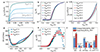 |
Figure 4 Electrical properties of undoped MoS2/MoTe2 JFET. (a) Output characteristics with increased gate voltage from 0 to 1 V. (b) Drain voltage dependent transfer characteristic curves. The current on-off ratio is about 105. (c) Linear plot of the transfer characteristics. The extracted pinch-off voltage VP is −0.18 V. (d) The SS extracted at three VDS of 1, 2, and 3 V. The minimum value of 113 mV dec−1 was extracted. (e) The gm as a function of gate voltage of the JFET at the VDS of 1, 2, and 3 V. (f) Multiple comparisons of key parameters of the uniformly doped and undoped MoS2/MoTe2 JFETs. |
CONCLUSIONS
In summary, we propose a uniform doping method for pre-depositing high-work-function Au under MoTe2 to optimize the performance of 2D MoS2/MoTe2 JFET. The JFET shows a near-ideal subthreshold swing of 62.5 mV dec−1 and an ultra-low gate leakage current of 10−12 A with MoS2 as the channel. The proposed JFET based on vdW p-n heterojunction performs better than previous studies in the same structure, especially in the subthreshold region, which proposes a promising way for future low-power electronic devices.
Data availability
The original data are available from corresponding authors upon reasonable request.
Acknowledgments
We are grateful to Yanlei Wang of Renmin University of China for constructive discussions. We are grateful to Yali Yang of University of Science and Technology Beijing for constructive discussions.
Funding
This work was supported by the National Natural Science Foundation of China (52350301, 52250398, 92463308, 62322402, 52188101, 52225206, 92163205, 62204012, 52303362, 62304019, 52302162 and 52402169), the National Key Research and Development Program of China (2022YFA1203803, 2024YFA1212600 and 2023YFF1500401), the Beijing Nova Program (20220484145 and 20230484478), the Young Elite Scientists Sponsorship Program by China Association for Science and Technology (2022QNRC001), the Fundamental Research Funds for the Central Universities (FRF-TP-22-004C2, FRF-06500207, FRF-TP-22-004A1, FRF-IDRY-22-016 and FRF-IDRY-23-038), the State Key Lab for Advanced Metals and Materials (2023-Z05), the Postdoctoral Fellowship Program of the China Postdoctoral Science Foudation (GZC20230233), and the special support from the Postdoctoral Science Foundation (2023TQ0007).
Author contributions
X.Z., Z.Z. and Y.Z. initiated and supervised the project. H.Y. and X.L. designed the research, analyzed the data, and wrote the manuscript. X.W. carried out the Raman and AFM measurement. Z.C. made revisions to the language of the manuscript. All authors have approved the final version of the manuscript.
Conflict of interest
The authors declare no conflict of interest.
Supplementary information
Supplementary file provided by the authors. Access Supplementary Material
References
- Zeng S, Liu C, Zhou P. Transistor engineering based on 2D materials in the post-silicon era. Nat Rev Electr Eng 2024; 1: 335-348. [Article] [Google Scholar]
- Cao W, Bu H, Vinet M, et al. The future transistors. Nature 2023; 620: 501-515. [Article] [Google Scholar]
- Zhang Q, Zhang Y, Luo Y, et al. New structure transistors for advanced technology node CMOS ICs. Natl Sci Rev 2024; 11: nwae008. [Article] [Google Scholar]
- Liu L, Chen Y, Chen L, et al. Ultrashort vertical-channel MoS2 transistor using a self-aligned contact. Nat Commun 2024; 15: 165. [Article] [Google Scholar]
- Pal A, Chavan T, Jabbour J, et al. Three-dimensional transistors with two-dimensional semiconductors for future CMOS scaling. Nat Electron 2024; 7: 1147-1157. [Article] [Google Scholar]
- Wang Y, Sarkar S, Yan H, et al. Critical challenges in the development of electronics based on two-dimensional transition metal dichalcogenides. Nat Electron 2024; 7: 638-645. [Article] [Google Scholar]
- Jazaeri F, Makris N, Saeidi A, et al. Charge-based model for junction FETs. IEEE Trans Electron Devices 2018; 65: 2694-2698. [Article] [Google Scholar]
- Chen X, Li S, Zhu L, et al. Dual-junction field-effect transistor with ultralow subthreshold swing approaching the theoretical limit. ACS Appl Mater Interfaces 2024; : acsami.3c17572. [Article] [Google Scholar]
- Shin HG, Kang D, Jeong Y, et al. High-performance van der Waals junction field-effect transistors utilizing organic molecule/transition metal dichalcogenide interface. ACS Nano 2020; 14: 15646-15653. [Article] [Google Scholar]
- Xu Y, Liu T, Liu K, et al. Scalable integration of hybrid high-κ dielectric materials on two-dimensional semiconductors. Nat Mater 2023; 22: 1078-1084. [Article] [Google Scholar]
- Li G, Qi J. Application and analysis on graphene materials. IOP Conf Ser-Earth Environ Sci 2018; 108: 022003. [Article] [Google Scholar]
- Wei X, Zhang X, Yu H, et al. Homojunction-loaded inverters based on self-biased molybdenum disulfide transistors for sub-picowatt computing. Nat Electron 2024; 7: 138-146. [Article] [Google Scholar]
- Jiang H, Zhang X, Chen K, et al. Two-dimensional czochralski growth of single-crystal MoS2. Nat Mater 2025; 24: 188-196. [Article] [Google Scholar]
- Hong M, Zhang X, Geng Y, et al. Universal transfer of full-class metal electrodes for barrier-free two-dimensional semiconductor contacts. InfoMat 2024; 6: e12491. [Article] [Google Scholar]
- Li F, Zeng J, Zhao Y, et al. High hole mobility van der Waals junction field-effect transistors based on Te/GaAs for multimode photodetection and logic applications. ACS Appl Mater Interfaces 2025; 17: 18655-18665. [Article] [Google Scholar]
- Wang H, Li Z, Li D, et al. Junction field-effect transistors based on PdSe2/MoS2 heterostructures for photodetectors showing high responsivity and detectivity. Adv Funct Mater 2021; 31: 2106105. [Article] [Google Scholar]
- Wang B, Wang L, Zhang Y, et al. Mixed-dimensional MoS2/Ge heterostructure junction field-effect transistors for logic operation and photodetection. Adv Funct Mater 2022; 32: 2110181. [Article] [Google Scholar]
- Zhang K, Li S, Chen J, et al. Dual-junctions field effect transistor based on MoS2/Te/MoS2. IEEE Trans Electron Devices 2023; 70: 3347-3353. [Article] [Google Scholar]
- Lim JY, Kim M, Jeong Y, et al. Van der Waals junction field effect transistors with both n- and p-channel transition metal dichalcogenides. npj 2D Mater Appl 2018; 2: 37. [Article] [Google Scholar]
- Wang Z, Xia H, Wang P, et al. Controllable doping in 2D layered materials. Adv Mater 2021; 33: 2104942. [Article] [Google Scholar]
- Yoo H, Heo K, Ansari MHR, et al. Recent advances in electrical doping of 2D semiconductor materials: Methods, analyses, and applications. Nanomaterials 2021; 11: 832. [Article] [Google Scholar]
- Zhang X, Kang Z, Gao L, et al. Molecule-upgraded van der Waals contacts for Schottky-barrier-free electronics. Adv Mater 2021; 33: 2104935. [Article] [Google Scholar]
- Yu H, Liao Q, Kang Z, et al. Atomic-thin ZnO sheet for visible-blind ultraviolet photodetection. Small 2020; 16: 2005520. [Article] [Google Scholar]
- Zhao Y, Gobbi M, Hueso LE, et al. Molecular approach to engineer two-dimensional devices for CMOS and beyond-CMOS applications. Chem Rev 2022; 122: 50-131. [Article] [Google Scholar]
- Zhang X, Liu B, Gao L, et al. Near-ideal van der Waals rectifiers based on all-two-dimensional Schottky junctions. Nat Commun 2021; 12: 1522. [Article] [Google Scholar]
- Zhao D, Chen Y, Jiang W, et al. Gate-tunable photodiodes based on mixed-dimensional Te/MoTe2 van der Waals heterojunctions. Adv Elect Mater 2021; 7: 2001066. [Article] [Google Scholar]
- Chen Y, Wang X, Wu G, et al. High-performance photovoltaic detector based on MoTe2/MoS2 van der Waals heterostructure. Small 2018; 14: 1703293. [Article] [Google Scholar]
- Huang M, Yu H, Wei X, et al. A 2D optoelectronic logic device with ultralow supply voltage. ACS Appl Mater Interfaces 2024; 16: 49620-49627. [Article] [Google Scholar]
- Song S, Keum DH, Cho S, et al. Room temperature semiconductor-metal transition of MoTe2 thin films engineered by strain. Nano Lett 2016; 16: 188-193. [Article] [Google Scholar]
- Li R, Hong M, Shangguan W, et al. Controlled lattice deformation for high-mobility two-dimensional MoTe2 growth. J Materiomics 2025; 11: 100868. [Article] [Google Scholar]
- Yu H, Wang Y, Zeng H, et al. High-spike barrier photodiodes based on 2D Te/WS2 heterostructures. ACS Nano 2024; 18: 17100-17110. [Article] [Google Scholar]
- Zhu L, Zhang J, Chen X, et al. Thinning solution-proceed 2D Te for p- and n-channel junction field effect transistor with high mobility and ideal subthreshold slope. Adv Funct Mater 2024; 34: 2316488. [Article] [Google Scholar]
- Yang Z, Liu X, Zou X, et al. Performance limits of the self-aligned nanowire top-gated MoS2 transistors. Adv Funct Mater 2017; 27: 1602250. [Article] [Google Scholar]
- Wang H, Li Y, Gao P, et al. Polarization- and gate-tunable optoelectronic reverse in 2D semimetal/semiconductor photovoltaic heterostructure. Adv Mater 2024; 36: 2309371. [Article] [Google Scholar]
All Figures
|
Figure 1 Comparisons of schematic diagrams, band structures and electrical properties between conventional and uniformly doped MoS2/MoTe2 JFET. (a, b) Schematic diagrams and atomic structures of the two JFETs. The red and green spheres represent MoS2, the blue and green spheres represent MoTe2, and the yellow spheres represent Au atoms. (c) The band diagrams of Au, MoTe2, and MoS2 before contact. (d, e) Band diagrams of the undoped (d) and Au-doped (e) MoS2/MoTe2 heterojunction. The ΔEV1 is the valence band offset when the MoS2/MoTe2 pn junction formed, which is about 0.6 eV. The ΔEV2 is the Schottky barrier height between Au and MoTe2, which is about 0.3 eV. The ΔEV3 is the valence band offset of the Au-doped MoS2/MoTe2 pn junction, while the ΔEV3 is approximately equal to ΔEV1 plus ΔEV2. (f) Transfer characteristics comparison with the VGS of 2 V. (g) The mobilities of undoped and doped JFETs with the VGS at 2 V. |
| In the text | |
|
Figure 2 Multi-angle comparisons of uniformly Au-doped and undoped MoTe2 FETs. (a) Optical image of the two MoTe2 FETs. (b) Drain voltage dependent transfer characteristic curves. (c) Raman curves of uniformly doped and undoped MoTe2. (d) Surface potential image of MoTe2 on Au and SiO2 substrates. (e) Potential line profile across the edge of the Au corresponding to the white line in (d). The inset is the optical microscope image of MoTe2 layer stack on the Au film and the insulating silicon substrate. (f) Band alignment of MoTe2/MoS2 heterojunction with the undoped MoTe2 (left) and the doped MoTe2 (right). (g) Rectification curves of doped and undoped MoS2/MoTe2 pn junction. (h) Band diagrams of the uniformly doped (blue) and undoped (grey) MoS2 along the channel length. |
| In the text | |
|
Figure 3 Electrical properties of Au-doped MoS2/MoTe2 JFET with MoS2 serves as channel material and MoTe2 serves as gate materials. (a) Optical microscope image of the MoS2/MoTe2 JFET. (b) Output characteristic curves of the MoS2/MoTe2 JFET. The three working stages represent (i) linear region, (ii) pinch-off region, and (iii) saturation region. (c) Drain voltage dependent transfer characteristic curves. (d) Linear plot of the transfer characteristic curves. The pinch-off voltage VP of the JFET is −0.10 V. (e) The SS extracted at different VDS at room temperature. (f) The gm as a function of gate voltage at the VDS of 1 and 2 V. (g–i) Cross-sectional view of the depletion region of the JFET at three stages of (g) linear region, (h) pinch-off region, and (i) saturation region, corresponding to the output characteristics in (b). The d represents the distance between the edge of the Au and MoS2 in the JFET. |
| In the text | |
|
Figure 4 Electrical properties of undoped MoS2/MoTe2 JFET. (a) Output characteristics with increased gate voltage from 0 to 1 V. (b) Drain voltage dependent transfer characteristic curves. The current on-off ratio is about 105. (c) Linear plot of the transfer characteristics. The extracted pinch-off voltage VP is −0.18 V. (d) The SS extracted at three VDS of 1, 2, and 3 V. The minimum value of 113 mV dec−1 was extracted. (e) The gm as a function of gate voltage of the JFET at the VDS of 1, 2, and 3 V. (f) Multiple comparisons of key parameters of the uniformly doped and undoped MoS2/MoTe2 JFETs. |
| In the text | |
Current usage metrics show cumulative count of Article Views (full-text article views including HTML views, PDF and ePub downloads, according to the available data) and Abstracts Views on Vision4Press platform.
Data correspond to usage on the plateform after 2015. The current usage metrics is available 48-96 hours after online publication and is updated daily on week days.
Initial download of the metrics may take a while.