Figure 3
Download original image
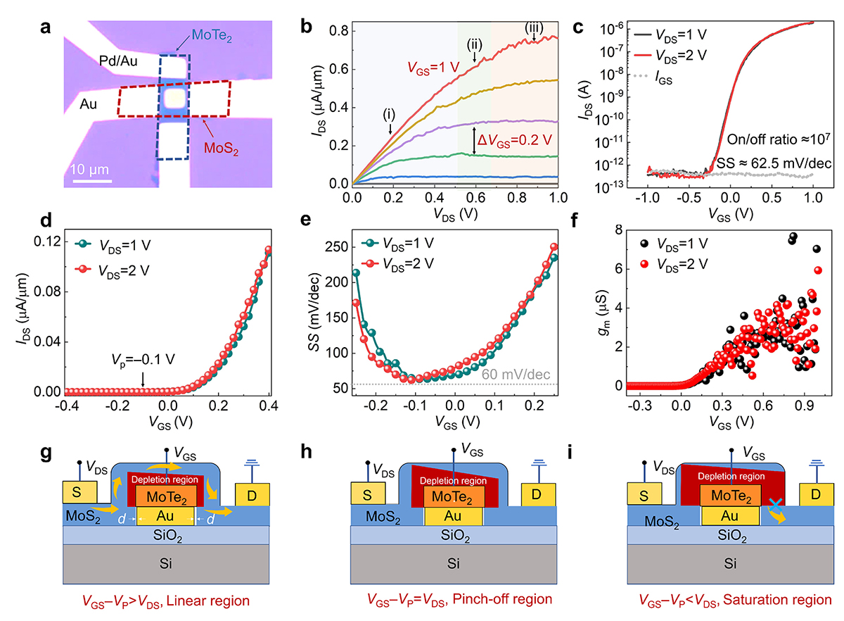
Electrical properties of Au-doped MoS2/MoTe2 JFET with MoS2 serves as channel material and MoTe2 serves as gate materials. (a) Optical microscope image of the MoS2/MoTe2 JFET. (b) Output characteristic curves of the MoS2/MoTe2 JFET. The three working stages represent (i) linear region, (ii) pinch-off region, and (iii) saturation region. (c) Drain voltage dependent transfer characteristic curves. (d) Linear plot of the transfer characteristic curves. The pinch-off voltage VP of the JFET is −0.10 V. (e) The SS extracted at different VDS at room temperature. (f) The gm as a function of gate voltage at the VDS of 1 and 2 V. (g–i) Cross-sectional view of the depletion region of the JFET at three stages of (g) linear region, (h) pinch-off region, and (i) saturation region, corresponding to the output characteristics in (b). The d represents the distance between the edge of the Au and MoS2 in the JFET.
Current usage metrics show cumulative count of Article Views (full-text article views including HTML views, PDF and ePub downloads, according to the available data) and Abstracts Views on Vision4Press platform.
Data correspond to usage on the plateform after 2015. The current usage metrics is available 48-96 hours after online publication and is updated daily on week days.
Initial download of the metrics may take a while.