Figure 2
Download original image
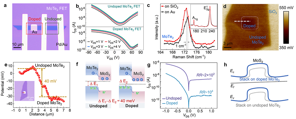
Multi-angle comparisons of uniformly Au-doped and undoped MoTe2 FETs. (a) Optical image of the two MoTe2 FETs. (b) Drain voltage dependent transfer characteristic curves. (c) Raman curves of uniformly doped and undoped MoTe2. (d) Surface potential image of MoTe2 on Au and SiO2 substrates. (e) Potential line profile across the edge of the Au corresponding to the white line in (d). The inset is the optical microscope image of MoTe2 layer stack on the Au film and the insulating silicon substrate. (f) Band alignment of MoTe2/MoS2 heterojunction with the undoped MoTe2 (left) and the doped MoTe2 (right). (g) Rectification curves of doped and undoped MoS2/MoTe2 pn junction. (h) Band diagrams of the uniformly doped (blue) and undoped (grey) MoS2 along the channel length.
Current usage metrics show cumulative count of Article Views (full-text article views including HTML views, PDF and ePub downloads, according to the available data) and Abstracts Views on Vision4Press platform.
Data correspond to usage on the plateform after 2015. The current usage metrics is available 48-96 hours after online publication and is updated daily on week days.
Initial download of the metrics may take a while.