| Issue |
Natl Sci Open
Volume 4, Number 3, 2025
Special Topic: Thermoelectric Materials and Devices
|
|
|---|---|---|
| Article Number | 20250006 | |
| Number of page(s) | 4 | |
| Section | Materials Science | |
| DOI | https://doi.org/10.1360/nso/20250006 | |
| Published online | 24 March 2025 | |
PERSPECTIVE
Electron microscopy approaches to thermoelectrics: Recent advances and emerging opportunities
Information Materials and Intelligent Sensing Laboratory of Anhui Province, Leibniz International Joint Research Center of Materials Sciences of Anhui Province, Institutes of Physical Science and Information Technology, Anhui University, Hefei 230601, China
* Corresponding authors (emails: This email address is being protected from spambots. You need JavaScript enabled to view it.
(Pengfei Nan); This email address is being protected from spambots. You need JavaScript enabled to view it.
(Binghui Ge))
Received:
25
February
2025
Revised:
15
March
2025
Accepted:
21
March
2025
Amid escalating global challenges in energy efficiency and environmental sustainability, the utilization of waste heat has gained significant scientific attention. This growing interest has positioned thermoelectric energy conversion as a pivotal research frontier in materials science, particularly for its potential to transform low-grade thermal energy into usable electricity. Thermoelectric materials hold significant potential in addressing this challenge due to their unique properties, such as the absence of vibration, radiation, and the ability to directly convert heat into electricity. The performance of thermoelectrics is assessed using the dimensionless thermoelectric figure of merit, zT, which is defined as

where S, σ, T, κE, and κL represent the Seebeck coefficient, electrical conductivity, absolute temperature, electronic thermal conductivity, and lattice thermal conductivity, respectively.
The enhancement of thermoelectric efficiency fundamentally relies on the optimization of critical performance parameters, among which κL plays a pivotal role. Recent advances in material engineering have demonstrated that strategic approaches including alloying [1], nanostructuring [2], and defect engineering [3] effectively suppress thermal transport by promoting phonon scattering through the introduction of defect structures at multiple length scales. Consequently, a deep understanding of the defect structures and their temporal evolution is essential for optimizing the performance of thermoelectric materials.
Within the spectrum of structural characterization methodologies, electron microscopy has emerged as an indispensable tool for establishing structure-property correlations in thermoelectric materials, primarily due to its unparalleled spatial resolution and comprehensive analytical versatility. Typically, high-resolution transmission electron microscopy (HRTEM) images are employed to identify various defect types, such as dislocations, grain boundaries, phase boundaries, twinning, and precipitates. Comprehensive information including elemental distribution, site occupancy, chemical shifts, electron orbital/spin and bonding, band gap, and valence states can be derived through energy dispersive X-ray spectroscopy and electron energy loss spectroscopy (EELS) [4]. Moreover, with the development of aberration-corrected techniques, annular bright field and integrated differential phase contrast technologies facilitate the simultaneous imaging of light and heavy atoms [5], while tomography techniques allow for the three-dimensional visualization of defect structures [6].
The advent of cutting-edge electron microscopy techniques has revolutionized our analytical capabilities, and extended well beyond the aforementioned applications, offering unprecedented opportunities to elucidate fundamental structure-property-performance relationships in thermoelectric systems. In the following sections, we present a comprehensive exploration of promising research directions that leverage these state-of-the-art microscopic approaches. (1) Employing high energy resolution EELS (Figure 1a) [7] to investigate phonon dispersion relationships of defects. This technique aids in understanding thermal conductivity and the interaction between phonons and electrons at the nanoscale, both of which are key factors influencing the efficiency of thermoelectric devices. (2) Easily thermal damaged samples such as fast ion conductors (e.g., Ag2S [8], Ag2Se) can be analyzed using cryogenic electron microscopy (cryo-EM) or aberration-corrected electron microscopy equipped with cryo-holders, or using low-dose and four-dimensional scanning transmission electron microscopy (4D-STEM) ptychography (Figure 1b) [9]. It is important to note that prior to utilizing cryogenic technology, it is necessary to employ alternative methods to confirm that the sample will not undergo a phase transition at low temperatures. (3) An in-situ chip integrated with micro-electrochemical systems (MEMS) may be capable of measuring the electrical properties of individual thermoelectric materials, including the Seebeck coefficient, electrical conductivity, and power factor (Figure 1c) [10]. The electrical conductivity σ can be calculated by the formula σ = IL/(ΔVA), where L represents the probe spacing, A denotes the cross-sectional area of the sample, I is the current, and ΔV is the potential difference. In contrast, the Seebeck coefficient S is determined by the ratio of voltage (ΔV) to temperature difference (ΔT), expressed as S = ΔV/ΔT. This approach can facilitate the correlation of thermoelectric properties with the structural and chemical composition of the thermoelectric materials at the atomic level, encompassing grain boundaries, dopants, or crystalline defects, while simultaneously tracking their dynamic evolution during heating or electric current application. (4) The advanced electron microscopy techniques discussed herein can be synergistically integrated to achieve comprehensive material characterization. Notably, the correlative approach combining EELS with ptychography enables simultaneous investigation of phonon dispersion characteristics and defect configurations. Furthermore, the integration of cryo-EM with ptychographic imaging offers a powerful solution for minimizing thermal artifacts while maintaining optimal electron dose conditions for defect structure analysis. Most significantly, the incorporation of in situ heating or electrical biasing capabilities with ptychographic techniques facilitates unprecedented opportunities for probing structural evolution under both static and dynamic thermal/electrical stimuli, thereby enabling real-time observation of material responses under operational conditions.
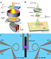 |
Figure 1 Working modes of new electron microscopy techniques. (a) Schematic of the 4D-EELS experimental setup for phonon dispersion curves, with a slot aperture placed parallel to the cBN-diamond interface, producing dispersion diagrams along the Γ-Σ-K-X high-symmetry line [7]. (b) Schematic of the 4D-STEM setup, where a convergent electron beam scans the sample point by point, collecting diffraction patterns to form a 4D-STEM dataset for ptychography [9]. (c) Schematic of the MEMS chip with eight electrical contacts for thermoelectric in-situ TEM characterization, with contacts for dual-probe electrical characteristics and two groups of heating elements and temperature sensors [10]. |
To date, state-of-the-art electron microscopy technologies have emerged as a transformative paradigm in thermoelectric materials research, establishing themselves as indispensable tools for elucidating the complex interplay between diverse defect configurations and their thermoelectric performance. This fundamental understanding at the atomic scale is revolutionizing our approach to materials design, enabling the rational development of next-generation thermoelectric systems with optimized performance characteristics and enhanced operational durability. Notably, these new techniques are currently at an idealized stage of application, and there is still a considerable distance before they can be practically applied to thermoelectric materials. Additionally, electron microscopy techniques for material characterization face limitations such as high costs, operational complexity, and challenges in sample preparation.
Funding
This work was supported by the National Key R&D Program of China (2022YFA1403203) and the National Natural Science Foundation of China (12474001).
Author contributions
P.N. and B.G. supervised the project. P.N. wrote the manuscript. All authors reviewed and edited the manuscript.
Conflict of interest
The authors declare no conflict of interest.
References
- Gayner C, Kar KK. Recent advances in thermoelectric materials. Prog Mater Sci 2016; 83: 330-382. [Article] [Google Scholar]
- Poudel B, Hao Q, Ma Y, et al. High-thermoelectric performance of nanostructured bismuth antimony telluride bulk alloys. Science 2008; 320: 634-638. [Article] [CrossRef] [PubMed] [Google Scholar]
- Zhou C, Lee YK, Cha J, et al. Defect engineering for high-performance n-type PbSe thermoelectrics. J Am Chem Soc 2018; 140: 9282-9290. [Article] [Google Scholar]
- Xie L, He D, He J. SnSe, the rising star thermoelectric material: A new paradigm in atomic blocks, building intriguing physical properties. Mater Horiz 2021; 8: 1847-1865. [Article] [Google Scholar]
- Nan P, Li A, Cheng L, et al. Visualizing the Mg atoms in Mg3Sb2 thermoelectrics using advanced iDPC-STEM technique. Mater Today Phys 2021; 21: 100524. [Article] [Google Scholar]
- Bals S, Casavola M, van Huis MA, et al. Three-dimensional atomic imaging of colloidal core-shell nanocrystals. Nano Lett 2011; 11: 3420-3424. [Article] [Google Scholar]
- Qi R, Shi R, Li Y, et al. Measuring phonon dispersion at an interface. Nature 2021; 599: 399-403. [Article] arxiv:2108.08904 [Google Scholar]
- Shi X, Chen H, Hao F, et al. Room-temperature ductile inorganic semiconductor. Nat Mater 2018; 17: 421-426. [Article] [Google Scholar]
- Li G, Zhang H, Han Y. 4D-STEM ptychography for electron-beam-sensitive materials. ACS Cent Sci 2022; 8: 1579-1588. [Article] [Google Scholar]
- Hettler S, Furqan M, Sotelo A, et al. Toward quantitative thermoelectric characterization of (nano)materials by in-situ transmission electron microscopy. Ultramicroscopy 2025; 268: 114071. [Article] [Google Scholar]
© The Author(s) 2025. Published by Science Press and EDP Sciences.
 This is an Open Access article distributed under the terms of the Creative Commons Attribution License (https://creativecommons.org/licenses/by/4.0), which permits unrestricted use, distribution, and reproduction in any medium, provided the original work is properly cited.
All Figures
|
Figure 1 Working modes of new electron microscopy techniques. (a) Schematic of the 4D-EELS experimental setup for phonon dispersion curves, with a slot aperture placed parallel to the cBN-diamond interface, producing dispersion diagrams along the Γ-Σ-K-X high-symmetry line [7]. (b) Schematic of the 4D-STEM setup, where a convergent electron beam scans the sample point by point, collecting diffraction patterns to form a 4D-STEM dataset for ptychography [9]. (c) Schematic of the MEMS chip with eight electrical contacts for thermoelectric in-situ TEM characterization, with contacts for dual-probe electrical characteristics and two groups of heating elements and temperature sensors [10]. |
| In the text | |
Current usage metrics show cumulative count of Article Views (full-text article views including HTML views, PDF and ePub downloads, according to the available data) and Abstracts Views on Vision4Press platform.
Data correspond to usage on the plateform after 2015. The current usage metrics is available 48-96 hours after online publication and is updated daily on week days.
Initial download of the metrics may take a while.