| Issue |
Natl Sci Open
Volume 4, Number 3, 2025
Special Topic: Thermoelectric Materials and Devices
|
|
|---|---|---|
| Article Number | 20250008 | |
| Number of page(s) | 10 | |
| Section | Materials Science | |
| DOI | https://doi.org/10.1360/nso/20250008 | |
| Published online | 11 April 2025 | |
RESEARCH ARTICLE
Achieving superior thermoelectric transport in bismuth antimony telluride thin films via orientation and microstructure regulation
1
School of Materials Science & Engineering, Beihang University, Beijing 100083, China
2
Key Laboratory of Intelligent Sensing Materials and Chip Integration Technology of Zhejiang Province, Hangzhou Innovation Institute of Beihang University, Hangzhou 310052, China
* Corresponding authors (emails: This email address is being protected from spambots. You need JavaScript enabled to view it.
(Weiyun Zhao); This email address is being protected from spambots. You need JavaScript enabled to view it.
(Yuan Deng))
Received:
14
March
2025
Revised:
5
April
2025
Accepted:
10
April
2025
Abstract
The electron-phonon transport properties of bismuth telluride-based thermoelectric materials are significantly influenced by crystallographic orientation and microstructure engineering. Thin-film materials are proper candidates for the study of structure-property relationship due to abundant microstructures. However, comprehensive studies on thin-film thermoelectric materials remain insufficient. Here, we synthesize p-type Bi0.5Sb1.5Te3 thin films via magnetron sputtering and followed by heat treatment. Preferential growth orientation of thin films exhibits a strong dependence on deposition conditions, allowing targeted orientation engineering through process parameter optimization. A high sputtering pressure of 3 Pa produces Bi0.5Sb1.5Te3 thin films with preferred in-plane orientation. The post-heat treatment enables precise regulation of electron-phonon coupling efficiency by engineering defect configurations. The dislocation density was reduced after annealing, and anti-site defects can also be tuned to optimized carrier concentration and mobility. After the heat annealing process under 400°C, a super high zT value of 1.49 was achieved at 313 K in Bi0.5Sb1.5Te3 thin film.
Key words: thermoelectric / bismuth antimony telluride / magnetron sputtering / microstructure / electron-phonon transport
© The Author(s) 2025. Published by Science Press and EDP Sciences.
 This is an Open Access article distributed under the terms of the Creative Commons Attribution License (https://creativecommons.org/licenses/by/4.0), which permits unrestricted use, distribution, and reproduction in any medium, provided the original work is properly cited.
INTRODUCTION
Thermoelectric (TE) material is a kind of functional material that can realize the mutual conversion of heat and electricity, playing an important role in the field of solid-state cooling and power generation [1–3]. The efficiency of TE materials is determined by figure of merit, zT = S2σT/κ, where S, σ, κ, and T are the Seebeck coefficient, electrical conductivity, thermal conductivity and absolute temperature, respectively. However, enhancing zT is challenged since the three parameters (S, σ, and κ) interact with each other. In recent years, more and more researchers have tried to decouple the contradiction of three parameters through regulating the structure and composition of the material [4–6].
In thin-film materials, the microstructures such as point defects, dislocations, grain boundaries and surfaces, is more abundant. Although these non-intrinsic factors bring great challenges to the quality of thin film, they also provide means for decoupling electrical and thermal transport. The point defects may affect the carrier concentration, mobility, density-of-state, effective mass and lattice thermal conductivity of the material [7–11]. The electrical conductivity and thermal conductivity can be controlled by forming dislocation array or adjusting dislocation density [11,12]. Grain boundaries can affect the migration of the carrier. It was found that the electrical conductivity of bulk materials can be enhanced by texture engineering [13]. Besides, by introducing atomic-scale point defects, nanocrystalline grains and mesoscale grain boundaries into thermoelectric materials, the thermal conductivity of the materials can be reduced to a great extent [14,15]. However, electroacoustic transport in relation to microstructures was mainly studied in bulk materials.
Bismuth telluride based material is one of the best and the only commercially used TE material at room temperature [16]. In this paper, we prepared a series of Bi0.5Sb1.5Te3 thin-film samples via magnetron sputtering and followed with heat treatment. The orientation of the films can be tunned by synthesis conditions. Our findings reveal that during the growth of Bi0.5Sb1.5Te3 crystals, the Te-rich (00l) surface becomes predominant under conditions that suppress Te evaporation. The microstructures were investigated via HRTEM (high-resolution transmission electron microscope) to the principle and technology of controlling defects in Bi0.5Sb1.5Te3 thin film at micro scale were studied. Hall measurements and thermoelectric parameters along in-plane direction of thin films were measured. And the relationships among scattering mechanism, electroacoustic transport mechanism and thermoelectric properties of thin films were discussed. With an optimized sputtering and heat treatment condition, a high zT value of 1.49 was achieved at 313 K.
MATERIALS AND METHODS
Thin film synthesis and thermal treatment
In this work, p-Bi0.5Sb1.5Te3 films were grown on AlN substrates at 400°C deposition temperature in a magnetron sputtering system (JGP-450a, SKY Technology Development Co., Ltd., Chinese Academy of Sciences). Before deposition, the AlN substrates were cleaned via ultrasonication in alcohol for 25 min, and then dried under the nitrogen airflow. Commercial purchased Bi0.5Sb1.5Te3 targets (99.99% purity, Qijin new material Technology Co., LTD, China) were used for sputtering. The Bi0.5Sb1.5Te3 target was connected to a direct-current (DC) power supply with a power of 10 W. The base pressure was lower than 1×10⁻³ Pa, and the working pressure of argon was fixed at 3 Pa. After sputtering for 2 h, the 300 nm-thick-TE film was obtained.
The films were annealed in a tubular furnace (Hefei Kejing OTF1200X). The samples were heated from room temperature to 300°C, 400°C, and 450°C respectively at a rate of 8°C/min, and after keeping the temperature for 20 min, the samples were cooled naturally. Argon gas was continuously injected into the tubular furnace during the annealing process.
Structure and morphology characterization
The crystal structures of the Bi0.5Sb1.5Te3 films were examined by X-ray diffraction (XRD, Rigaku D/MAX 2200). The film morphology and thickness were observed by field emission scanning electron microscopy (FE-SEM, FEI Sirion 200). The compositions were detected by energy dispersive spectrometer (EDS). The micro-structure of the films was detected by the high resolution transmission electron microscope (TEM, Talos F200X G2).
Thermoelectric properties measurement
The carrier concentration and mobility were measured using a four-probe measurement based on the Hall effects (NanoMagnetics, ezHEMS500). The electrical conductivity, the Seebeck coefficient and the power factor were measured on the CTA-3 Seebeck coefficient and resistivity tester (CTA, Beijing Cryall Technology Co., LTD). The in-plane thermal conductivity was measured via 3-omega (3ω) method on the film thermal conductivity tester (TFA, LINSEIS Messgeräte GmbH.). The parameters mentioned above are all measured at temperatures of 313, 353, 393, 433, 473 and 513 K.
RESULTS AND DISCUSSION
Bi2Te3 based materials have layered structure and show anisotropic electrical and thermal properties. We first synthesized Bi0.5Sb1.5Te3 thin films by magnetron sputtering and investigated the influence of synthesis conditions on film orientation. The magnetron sputtering method can be used to precisely control the macro-scale properties of the prepared films such as grain size, film thickness and film density by adjusting the sputtering parameters [17,18]. Here, we focused more attention on the orientation of the film. The energy competition during the deposition process may determine the main orientation of the film. Usually, the Bi0.5Sb1.5Te3 crystal will grow along the low surface energy direction such as (00l) and (015), which are along the slipping path [19]. We tunned the deposition pressure from 1.5 to 3 Pa, and found that the orientations of the films were especially sensitive to the pressure (Figure 1a). (00l) direction has the lowest surface energy, but (015) is the dominant direction when pressure is 1.5 and 2 Pa. When the film grows along (015), the in-plane stress can be released through (00l) slipping path. With the increase of pressure, the peaks corresponding to (00l) became stronger. The film grew under 3 Pa pressure exhibited most obvious (00l) direction. The deposition pressure can directly influence the chemical potential of elements, thereby modifying thermodynamic equilibrium. The increased pressure inhibits the evaporation of Te, thereby favoring the formation of Te-rich (00l) surfaces (Figure 1b) [20]. This structural configuration promotes the transport of electrons, potentially enhancing the material’s electrical conductivity. Hence, in order to enhance the in-plane transport of thin films, the pressure we used in all the subsequent synthesis was 3 Pa.
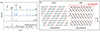 |
Figure 1 (a) XRD pattern of Bi0.5Sb1.5Te3 prepared under different pressures. (b) The atomic structure of (015) and (00l) direction constructed using VESTA [20], showing Te-rich surface of (00l) direction. |
The temperature also can further tunning the orientation as well as microstructure of Bi0.5Sb1.5Te3 thin films. We did heat treatments on all the as-prepared Bi0.5Sb1.5Te3 thin films via annealing in the tube furnace. Although magnetron sputtering has already determined the orientation of crystals, there is a difference in orientation between the bottom and surface of the thin films generated during the sputtering deposition process. This phenomenon arises because as the deposition thickness increases, internal stress within the film is gradually released through dislocation glide, leading to a deviation in the orientation of surface grains. Then, the annealing process promotes continuous grain growth and refines grain orientation by facilitating crystallographic. Therefore, SEM images (Figure 2a‒d) showing the surface morphology of thin films, exhibit quite different morphologies. With the increase of annealing temperature, the tendency of laminar growth becomes more obvious. It can be seen from Figure S1 that with the increase of annealing temperature, the thickness of the film decreases slightly while the density increases gradually. The XRD patterns in Figure 2e confirm that the crystallinity of the sample was improved after annealing at 400°C. And although the main growth directions of the film before and after annealing are both (00l), the tendency is much more obvious in the film after annealing. We compared the full width at half maxima (FWHM) of as-prepared and annealed Bi0.5Sb1.5Te3 thin films. The smaller FWHM value of annealed sample proved that the grain size grew bigger after annealed. Therefore, it is speculated that Bi0.5Sb1.5Te3 recrystallized during the heat treatment process, which increased the crystallinity of Bi0.5Sb1.5Te3, made the grain growth direction more inclined to (00l), and changed the microstructure of the material. It is worth mentioning that the improvement of crystallinity and the transformation of crystal direction to (00l) are conducive to the improvement of the conductivity. Since  , where L is the grain size, q is the amount of charge of a carrier, m* is the effective mass and ϕb is the grain boundary barrier. μ is negatively correlated with ϕb, which is related to grain boundary inclination. The larger the disorientation angle, the higher the barrier height. Therefore, the preferred orientation is beneficial to reduce grain boundary scattering, thus enhancing the carrier mobility. Furthermore, the preferential growth of (00l) plane is beneficial for the increase of carrier mobility and electron scattering parameter, which brings higher electrical conductivity than those of films with preferential growth of (015) plane [21].
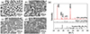 |
Figure 2 The SEM image of the Bi0.5Sb1.5Te3 thin film before and after annealing. (a) As-prepared Bi0.5Sb1.5Te3 thin film without annealing; annealed Bi0.5Sb1.5Te3 thin film at (b) 300°C, (c) 400°C, and (d) 450°C. (e) The XRD patterns of Bi0.5Sb1.5Te3 thin film before and after annealing at 400°C. |
To explore the defect evolution mechanism in thermal processing, we used TEM to characterize the material microstructures (Figure 3). Figure 3a and d are the typical Bi0.5Sb1.5Te3 crystal of as-prepared thin film and annealed thin film. Figure 3b and e are the enlarged figures showing lattice structures of thin films before and after annealing. By comparing two figures, it can be clearly seen that the crystallinity of the annealed material is improved, which is consistent with the XRD results. Figure 3c and f are the corresponding iFFT (inverse fast Fourier transform) images of Figure 3b and e. It can be found that there are a large number of dislocation structures in the material before annealing. We denoted some in Figure 3c by red marks. However, after annealing, the amount of dislocation is significantly reduced as shown in Figure 3f. This phenomenon indicates that proper thermal treatment helps to reduce dislocation density, and it may enhance the transportation of carriers. At the same time, we also find that the lattice distortion structures were maintained after the annealing process shown in Figure S2.
 |
Figure 3 The TEM pattern of p-Bi0.5Sb1.5Te3 before and after annealing. (a) Lattice of the sample before annealing. (b) A larger view of the area in the box in (a) and its FFT image. (c) The iFFT image corresponding to the box area in (a). (d) Lattice of the sample after annealing. (e) A larger view of the area in the box in (d) and its FFT image. (f) The iFFT image corresponds to the box area in (d). |
After confirming that heat treatment can effectively regulate the microstructure of the material, the optimal annealing temperature was further explored. Herein the Bi0.5Sb1.5Te3 film was annealed under 300°C, 350°C, 400°C, and 450°C (denoted as BST-300, BST-350, BST-400, and BST-450, respectively), and Hall as well as TE properties measurements were conducted. Considering the film direction and anisotropy of the thin films, we measured all the parameters along in-plane direction. We first used hall measurements to clarify the influence of the heat treatment process to the carrier concentration and mobility, which is quite important to the thermoelectric properties. Figure 4a is the carrier concentration of all the prepared thin films. The films annealed at lower temperature (i.e., BST-300 and BST-350) have lower carrier concentration compared to that of as-prepared film. When the annealed temperature increased to 400°C and 450°C, the carrier concentration became larger. The intrinsic point defects such as vacancies, anti-site defects existed in Bi0.5Sb1.5Te3 film can be engineered during the heat treatment process [10]. Lower annealing temperature, such as 300°C or 350°C in this work, can eliminate some anti-site defects TeBi. With the increase of annealing temperature, more Te vacancy was generated as Te evaporated (Table S1). When the annealing temperature increased to 400°C or 450°C, new anti-site defects generated due to the transformation of Te vacancies to anti-sites defects BiTe [22], and hence the carrier concentration increased again.
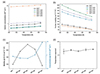 |
Figure 4 Hall measurements results of all the samples. (a) Carrier concentration. (b) Carrier mobility. (c) The influence of annealing temperature on carrier mobility and concentration measured at 313 K. (d) The corresponding exponent α for μ ∝ Tα at 313 K. |
The carrier mobility of all the thin films were shown in Figure 4b. With the annealing temperature continuously increasing, carrier mobility increased first and then decreased. Carrier mobility is mainly influenced by carrier scattering. We further used the carrier mobility at 313 K to derived exponent α for μ ∝ Tα at 313 K (Figure 4c and d). The value of exponent α is in the range of −0.5‒−1 for all the samples, indicating that both carrier-phonon scattering and carrier-defect scattering exist in the materials [23]. Although both phonons and defects can scatter carriers, carrier-phonon scattering is the intrinsic properties, which is expected to remain unchanged with different annealing temperatures. Hence we focus on the carrier-defect scattering here. As we have discussed in the carrier concentration part, lower annealing temperature eliminates some defects such as TeBi, and higher annealing temperature caused more Te vacancy as well as BiTe. The amount of defects decreased first and then increased with the annealing temperature. Therefore, the mobility increased first and then decreased.
The results of Hall measurements already reveal the influence caused by orientation and defects. The carrier concentration and mobility jointly influence the electrical conductivity of Bi0.5Sb1.5Te3. Therefore the correlation of electron transport through processing condition is further clarified via in-plane electrical conductivities measurements (Figure 5a). After annealing, the conductivity of thin films was improved. With the increase of annealing temperature, the conductivity of the material increased obviously due to less defects and higher in-plane orientation. The conductivity variation trends with measured temperatures are different between samples and depend on the annealing temperature. When the annealing temperature is 300°C and 350°C, the conductivity of the film increases with the increase of temperature. This is because BST-300 and BST-350 have lower carrier concentration, thus the bipolar transport effect is more significant at higher temperature due to thermal activation of electrons in conduction band. BST-400 and BST-450 have higher carrier concentration, so the bipolar effect becomes less important. The increase in temperature will promote the thermal motion of atoms and the electron-phonon scattering was intensified, thereby leading to the reduction of conductivity at higher temperature.
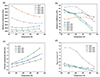 |
Figure 5 Thermoelectric properties of Bi0.5Sb1.5Te3 samples annealed at different temperatures. (a) Electrical conductivity of samples annealed at different temperatures. (b) Seebeck coefficient of samples annealed at different temperatures. (c) Thermal conductivity of samples annealed at different temperatures. (d) Power factor of samples annealed at different temperatures. |
Seebeck coefficient also exhibits strong correlation with electron transport. Figure 5b shows how the Seebeck coefficients of the above groups change with temperature. The sample BST was not annealed, which means it’s thermodynamically unstable. Therefore, its Seebeck coefficient fluctuates slightly with the change of test temperature. The Seebeck coefficients of BST-300, BST-350, and BST-400 decrease rapidly with the increase of test temperature, which may be caused by bipolar effect. However, the Seebeck coefficient of BST-450 does not change as sharply with temperature as the previous three groups in the test temperature range, which may be due to the volatilization of Te element and the increase of Te vacancy caused by high temperature annealing, forming the reverse position defect of Bi taking the Te position. This increases the number of p-type carriers and weakens the bipolar effect. Therefore, the variation trend of the material’s power factor with annealing temperature is basically the same as that of its conductivity with annealing temperature.
The previous works on phonon transport in thin film samples are quite limited, owing to the challenge on thermal properties measurements at reduced dimensions. Here, we conducted thermal conductivity measurements of thin films via 3ω method (Figure S3), which is a way to measure in-plane thermal conductivity of thin film sample [24]. The films were deposited and annealed directly on the commercial testing chips from Linseis. Since the testing chip can be spoiled under high annealing temperature, we only tested thermal conductivity of BST, BST-300, BST-350, and BST-400 at different temperatures (Figure 5c). As we mentioned, the lattice distortion structures (Figure S2) were maintained after annealing, and lead a strong phonon scattering. Hence, all the films, including both as-prepared and annealed, have very low thermal conductivity. The increase of electrical conductivity after annealing resulted in an increase in electronic thermal conductivity. The thermal conductivity of the annealed film is inevitably higher than that of the as-prepared BST.
Collated the measured electrical conductivity, Seebeck coefficient and thermal conductivity results, figure of merit zT of the thin films is calculated (Figure 5d). The thermoelectric value of BST-400 was significantly higher than that of the other films at all the measured temperatures. The coordinated orientation engineering via magnetron sputtering and defect configuration optimization through post-annealing synergistically enhance the thermoelectric performance of BST-400. The enhancement manifests high electrical conductivity due to the dominated orientation of (00l) and reduced dislocation density, high Seebeck coefficient due to a proper carrier concentration, as well as low thermal conductivity due to strong phonon scattering from lattice distortion. Combine all the parameters, a highest zT value of BST-400 achieved to 1.49 at 313 K.
CONCLUSIONS
In conclusion, we demonstrates an orientation and microstructure engineering strategy for Bi0.5Sb1.5Te3 thin films through synergistic control of sputtering parameters and post-annealing processes. We found that the orientation of Bi0.5Sb1.5Te3 thin film is sensitive to the synthesis pressure, and it is easier to form in-plane growth under higher pressure (3 Pa). The heat treatment process can further enhance the in-plane orientation of the film. Moreover, the density of dislocation was sensitive to the annealing temperature, while the lattice distortion structure can be maintained after our annealing process. The carrier concentration was also influenced by heat treatment process. The hall measurements indicated that the amount of anti-site defects was affected by annealing temperature. All the thermoelectric properties of thin films were measured along in-plane direction. The reduced amount of dislocation achieved high electrical conductivity, and meanwhile, lattice distortion led a strong phonon scattering to keep low thermal conductivity. A high zT value of 1.49 was achieved after fine-tuning the Bi0.5Sb1.5Te3 thin film microstructures in this work.
Data availability
The original data are available from corresponding authors upon reasonable request.
Funding
This work was supported by the National Natural Science Foundation of China (52102202).
Author contributions
Y.Q. and W.Z. designed the research and analyzed the data. Y.Q. did the experiments and characterizations. B.Z. performed some experiments. Y.Q. wrote the manuscript. W.Z. and Y.D. modified the manuscript.
Conflict of interest
The authors declare no conflict of interest.
Supplementary information
Supplementary file provided by the authors. Access Supplementary Material
The supporting materials are published as submitted, without typesetting or editing. The responsibility for scientific accuracy and content remains entirely with the authors.
References
- Poudel B, Hao Q, Ma Y, et al. High-thermoelectric performance of nanostructured bismuth antimony telluride bulk alloys. Science 2008; 320: 634-638. [Article] [CrossRef] [PubMed] [Google Scholar]
- Tritt TM, Böttner H, Chen L. Thermoelectrics: Direct solar thermal energy conversion. MRS Bull 2008; 33: 366-368. [Article] [Google Scholar]
- Chowdhury I, Prasher R, Lofgreen K, et al. On-chip cooling by superlattice-based thin-film thermoelectrics. Nat Nanotech 2009; 4: 235-238. [Article] [Google Scholar]
- Hu L, Wu H, Zhu T, et al. Tuning multiscale microstructures to enhance thermoelectric performance of n-type bismuth-telluride-based solid solutions. Adv Energy Mater 2015; 5: 1500411. [Article] [CrossRef] [Google Scholar]
- Chang C, Wu M, He D, et al. 3D charge and 2D phonon transports leading to high out-of-plane ZT in n-type SnSe crystals. Science 2018; 360: 778-783. [Article] [Google Scholar]
- Su L, Wang D, Wang S, et al. High thermoelectric performance realized through manipulating layered phonon-electron decoupling. Science 2022; 375: 1385-1389. [Article] [Google Scholar]
- Li S, Fang X, Lyu T, et al. Antisite defect manipulation enables the high thermoelectric performance of p-type Bi2−xSbxTe3 alloys for solid-state refrigeration. Mater Today Phys 2022; 27: 100764. [Article] [Google Scholar]
- Starý Z, Horák J, Stordeur M, et al. Antisite defects in Sb2−xBixTe3 mixed crystals. J Phys Chem Solids 1988; 49: 29-34. [Article] [Google Scholar]
- Hu L, Zhu T, Liu X, et al. Point defect engineering of high-performance bismuth-telluride-based thermoelectric materials. Adv Funct Mater 2015; 24: 5211-5218. [Article] [Google Scholar]
- Wang Y, Liu WD, Shi XL, et al. Enhanced thermoelectric properties of nanostructured n-type Bi2Te3 by suppressing Te vacancy through non-equilibrium fast reaction. Chem Eng J 2020; 391: 123513. [Article] [Google Scholar]
- Chen Z, Ge B, Li W, et al. Vacancy-induced dislocations within grains for high-performance PbSe thermoelectrics. Nat Commun 2017; 8: 13828. [Article] [CrossRef] [PubMed] [Google Scholar]
- Kim SI, Lee KH, Mun HA, et al. Dense dislocation arrays embedded in grain boundaries for high-performance bulk thermoelectrics. Science 2015; 348: 109-114. [Article] [Google Scholar]
- Shen JJ, Hu LP, Zhu TJ, et al. The texture related anisotropy of thermoelectric properties in bismuth telluride based polycrystalline alloys. Appl Phys Lett 2011; 99: 124102. [Article] [CrossRef] [Google Scholar]
- Biswas K, He J, Blum ID, et al. High-performance bulk thermoelectrics with all-scale hierarchical architectures. Nature 2012; 489: 414-418. [Article] [CrossRef] [PubMed] [Google Scholar]
- Hu L, Gao H, Liu X, et al. Enhancement in thermoelectric performance of bismuth telluride based alloys by multi-scale microstructural effects. J Mater Chem 2012; 22: 16484-16490. [Article] [Google Scholar]
- Pang K, Miao L, Zhang Q, et al. Gradient nanotwins and enhanced weighted mobility synergistically upgrade Bi0.5Sb1.5Te3 thermoelectric and mechanical performance. Adv Funct Mater 2024; 34: 2315591. [Article] [CrossRef] [Google Scholar]
- Fan P, Li R, Chen YX, et al. High thermoelectric performance achieved in Bi0.4Sb1.6Te3 films with high (00l) orientation via magnetron sputtering. J Eur Ceram Soc 2020; 40: 4016-4021. [Article] [Google Scholar]
- Qiu G, Li J, Ling Y, et al. Carrier concentration and orientation optimization for high performance (Sb,Bi)2Te3 thermoelectric films via magnetron co-sputtering. J Alloys Compd 2023; 950: 169916. [Article] [Google Scholar]
- Deng T, Gao Z, Li Z, et al. Room-temperature exceptional plasticity in defective Bi2Te3-based bulk thermoelectric crystals. Science 2024; 386: 1112-1117. [Article] [Google Scholar]
- Momma K, Izumi F. VESTA 3 for three-dimensional visualization of crystal, volumetric and morphology data. J Appl Crystlogr 2011; 44: 1272-1276. [Article] [Google Scholar]
- Deng Y, Zhang Z, Wang Y, et al. Preferential growth of Bi2Te3 films with a nanolayer structure: Enhancement of thermoelectric properties induced by nanocrystal boundaries. J Nanopart Res 2012; 14: 775. [Article] [Google Scholar]
- Zhang M, Liu W, Zhang C, et al. Identifying the manipulation of individual atomic-scale defects for boosting thermoelectric performances in artificially controlled Bi2Te3 films. ACS Nano 2021; 15: 5706-5714. [Article] [Google Scholar]
- Goldsmid HJ. Thermoelectric properties of metals and semiconductors. In: Introduction to Thermoelectricity. Berlin, Heidelberg: Springer, 2016, 25–44 [Google Scholar]
- Dames C. Measuring the thermal conductivity of thin films: 3 omega and related electrothermal methods. Annu Rev Heat Transfer 2012; 16: 7-49. [Article] [Google Scholar]
All Figures
|
Figure 1 (a) XRD pattern of Bi0.5Sb1.5Te3 prepared under different pressures. (b) The atomic structure of (015) and (00l) direction constructed using VESTA [20], showing Te-rich surface of (00l) direction. |
| In the text | |
|
Figure 2 The SEM image of the Bi0.5Sb1.5Te3 thin film before and after annealing. (a) As-prepared Bi0.5Sb1.5Te3 thin film without annealing; annealed Bi0.5Sb1.5Te3 thin film at (b) 300°C, (c) 400°C, and (d) 450°C. (e) The XRD patterns of Bi0.5Sb1.5Te3 thin film before and after annealing at 400°C. |
| In the text | |
|
Figure 3 The TEM pattern of p-Bi0.5Sb1.5Te3 before and after annealing. (a) Lattice of the sample before annealing. (b) A larger view of the area in the box in (a) and its FFT image. (c) The iFFT image corresponding to the box area in (a). (d) Lattice of the sample after annealing. (e) A larger view of the area in the box in (d) and its FFT image. (f) The iFFT image corresponds to the box area in (d). |
| In the text | |
|
Figure 4 Hall measurements results of all the samples. (a) Carrier concentration. (b) Carrier mobility. (c) The influence of annealing temperature on carrier mobility and concentration measured at 313 K. (d) The corresponding exponent α for μ ∝ Tα at 313 K. |
| In the text | |
|
Figure 5 Thermoelectric properties of Bi0.5Sb1.5Te3 samples annealed at different temperatures. (a) Electrical conductivity of samples annealed at different temperatures. (b) Seebeck coefficient of samples annealed at different temperatures. (c) Thermal conductivity of samples annealed at different temperatures. (d) Power factor of samples annealed at different temperatures. |
| In the text | |
Current usage metrics show cumulative count of Article Views (full-text article views including HTML views, PDF and ePub downloads, according to the available data) and Abstracts Views on Vision4Press platform.
Data correspond to usage on the plateform after 2015. The current usage metrics is available 48-96 hours after online publication and is updated daily on week days.
Initial download of the metrics may take a while.