| Issue |
Natl Sci Open
Volume 4, Number 3, 2025
Special Topic: Thermoelectric Materials and Devices
|
|
|---|---|---|
| Article Number | 20250004 | |
| Number of page(s) | 18 | |
| Section | Materials Science | |
| DOI | https://doi.org/10.1360/nso/20250004 | |
| Published online | 25 March 2025 | |
RESEARCH ARTICLE
Off-centering effect and crystal symmetry modification lead to high thermoelectric performance in diamondoid Cu2SnSe3
1
School of Materials Science and Engineering, Beihang University, Beijing 100191, China
2
Center for Bioinspired Science and Technology, Hangzhou International Innovation Institute, Beihang University, Hangzhou 311115, China
3
State Key Laboratory of Advanced Technology for Materials Synthesis and Processing, Wuhan University of Technology, Wuhan 430070, China
4
Center for High Pressure Science and Technology Advanced Research (HPSTAR), Beijing 100094, China
* Corresponding authors (emails: This email address is being protected from spambots. You need JavaScript enabled to view it.
(Hongyao Xie); This email address is being protected from spambots. You need JavaScript enabled to view it.
(Li-Dong Zhao))
Received:
13
February
2025
Revised:
13
March
2025
Accepted:
24
March
2025
Abstract
Recently, dimensionless figure of merit (ZT) beyond 1.0 has been demonstrated in diamondoid Cu2SnSe3, positioning it as a low-cost and ecofriendly thermoelectric alternative, and sparking intense interest in further optimizing its thermoelectric properties. However, its intrinsic monoclinic structure and the compact packing of tetrahedral coordination lead to a light valence band and high thermal conductivity, which impede further performance improvement in Cu2SnSe3. Thus, developing effective approaches to altering the local structure of Cu2SnSe3 is important for further optimizing its thermoelectric performance. Herein, we identified and thoroughly investigated the atomic off-centering behavior in Cu2SnSe3, and demonstrated the electronic and phonon transport properties of Cu2SnSe3 can be significantly enhanced by carefully modifying its monoclinic lattice into a distorted zinc-blende cubic structure via introducing Cd and off-centering Ag elements. This structure transition leads to band convergence and a reduction in the deformation potential of the material, resulting in a 7-fold enhancement in the density-of-state effective mass and an 85% increase in carrier mobility. Additionally, the off-centering effect results in strong acoustic-optical phonon scattering and an ultra-low lattice thermal conductivity of 0.3 W m−1 K−1. Consequently, a maximum ZT of 1.3 was obtained at 800 K for the Cu1.85Ag0.15Sn0.9Cd0.1Se3.
Key words: thermoelectric / crystal structure transition / off-centering behavior / local symmetry breaking
Contributed equally to this work.
© The Author(s) 2025. Published by Science Press and EDP Sciences.
 This is an Open Access article distributed under the terms of the Creative Commons Attribution License (https://creativecommons.org/licenses/by/4.0), which permits unrestricted use, distribution, and reproduction in any medium, provided the original work is properly cited.
INTRODUCTION
Thermoelectric materials facilitate the direct and reversible conversion between heat and electrical energy, making them suitable for applications in solid-state refrigeration and waste heat recovery [1]. The thermoelectric performance of a material is quantified by the dimensionless figure of merit (ZT) [2–4]:
 (1)
(1)
where S is the Seebeck coefficient, σ denotes electrical conductivity, T represents the Kelvin temperature, and  is total thermal conductivity, which includes electronic (
 ) and lattice (
 ) contributions. Outstanding thermoelectric materials usually require a high power factor (PF = S2σ) and a low thermal conductivity. However, all these transport properties are interconnected via the electronic band structure and carrier concentration, except for the lattice thermal conductivity, which depends solely on phonon vibration. Therefore, optimizing these thermoelectric parameters presents a significant challenge, which can be addressed through the synergistic enhancement of electronic transport properties and the suppression of phonon vibration [5,6]. Numerous efforts have been made and a variety of strategies have been developed, including lattice plainification [7–9], multi-band synglisis [10], nanostructuring [11], entropy engineering [12,13] and atomic off-centering [14,15], to name just a few.
For a long time, wide band gap semiconductors were avoided for thermoelectric applications, since their relatively low electrical conductivity, and most traditional thermoelectric materials are narrow band gap semiconductors, such as Bi2Te3 [16,17], PbQ (Q = S, Se, Te) [18–21], GeTe [22,23], SnTe [24,25], Zintl phases [26,27], and filled-skutterudites [28,29]. Until recently, it has been observed that wide band gap thermoelectric materials typically exhibit a high Seebeck coefficient and lack bipolar behavior, enabling them to function effectively over a broad temperature range without intrinsic excitation. Inspired by this, several novel high-performance wide band gap thermoelectric materials have been developed, including SnSe [30,31], SnS [32,33], Cu2Se [34], and Mg3(Sb,Bi)2 [35]. These advancements have absorbed significant attention in investigating other wide band gap thermoelectric semiconductors. Ternary diamondoid compounds represent a substantial group of wide band gap semiconductors, encompassing families such as I2-IV-VI3 and I-III-VI2 families (I = Cu, Ag; III = Al, Ga, In; IV = Si, Ge, Sn; VI = S, Se, Te). These materials originate from a diamond structure and exhibit tetrahedral coordination, which is classified as diamondoid compounds. Due to the relatively wide band gaps, diamondoid compounds have historically received considerable attention in the solar cells and photocatalysis fields [4]. However, recent reports show that ZT beyond 1.0 can be achieved in many diamondoid materials, such as Cu(In, Ga)Te2 [36–38], AgInSe2 [39], Cu2SnSe3 [40,41], Cu3SbSe4 [42] and Cu2ZnSnS4 [43], demonstrating the immense potential of diamondoid compounds for thermoelectric application.
Among them, the diamondoid Cu2SnSe3 compound attracted significant attention due to its adjustable electrical conductivity, inexpensive and abundant constituent elements, as well as relatively high mechanical properties [44]. The p-type Cu2SnSe3 compound features a direct electronic band gap (Eg) of 0.85 eV [45]. Because of the abundant Cu vacancies [46,47], intrinsic Cu2SnSe3 possesses a high carrier concentration of approximately 1019 cm−3, and this value can be easily regulated due to its dopability. However, intrinsic Cu2SnSe3 has a low-symmetry monoclinic structure, which leads to a light valence band and a low density-of-states effective mass. The large electronegativity difference between the cations and anions also results in strong ionic bonding and a low carrier mobility (μ) less than 10 cm2 V−1 s−1 [41]. Moreover, the compact packing of tetrahedral coordination and the strong chemical bonding result in a relatively high intrinsic  of 2.7 W m−1 K−1 at room temperature [46]. All these are the critical challenges in enhancing the thermoelectric performance of diamondoid Cu2SnSe3. Therefore, revealing the influence of lattice dynamics on the electronic and phonon transport properties of Cu2SnSe3, and developing effective strategies to alter its local structure is essential for further optimizing its thermoelectric performance.
Introducing external tetrahedral compounds could be an effective way to alter the local crystal structure and transport properties of Cu2SnSe3. Upon reviewing other homologous diamondoid compounds, we found that the zinc blende CdSe exhibits a high μ of 660 cm2 V−1 s−1 [48]. Introducing Cd into the Cu2SnSe3 matrix to form Cd-Se4 tetrahedra may enhance carrier mobility and promote carrier transport. Furthermore, our recent study showed that the Ag atom exhibits significant off-centering behavior within the tetrahedral structure [49], which leads to intense acoustic-optical phonon scattering and a low intrinsic lattice thermal conductivity in the diamondoid AgGaTe2 compound. The off-centering nature of Ag atoms arises from weakened sd3 orbital hybridization, which is electronic in origin and is expected to be observed in other Ag-based diamondoid materials. Thus, alloying Ag into Cu2SnSe3 to form Ag-Se4 tetrahedra may introduce similar phonon coupling in Cu2SnSe3, thereby reducing the thermal conductivity of the system. Inspired by these considerations, in this work, we synthesized Cd and Ag co-doped Cu2SnSe3 and investigated the effects of these elements on the local structure, as well as the electronic and heat transport essence of Cu2SnSe3, with the goal of extending this optimization strategy to other diamondoid systems.
We found that substituting Sn with Cd is able to promote the transformation of Cu2SnSe3 from an intrinsic monoclinic structure to a cubic zinc blende crystal structure (Figure 1a). This structural transition leads to valence band convergence and significantly increases the density-of-states effective mass from 0.2me to 1.4me. Moreover, both the structural transition and Cd doping lower the deformation potential, which effectively increases the μ from 11.5 to 21.3 cm2 V−1 s−1. Meanwhile, replacing Sn4+ with Cd2+ significantly increases the carrier concentration of Cu2SnSe3, see Figure 1b and d. This combined improvement in carrier concentration and mobility dramatically raises the PF of the material from ~1.5 to ~13 μW cm−1 K−2 at 773 K. Furthermore, introducing off-centering Ag into Cu2SnSe3 distorts the Se4 tetrahedral coordination structure and leads to local symmetry breaking in the material, thereby reducing sound velocity and Debye temperature, see Figure 1c, e. We reveal that the off-centering Ag originates from weakened sd3 orbital hybridization, inducing strong phonon scattering between heat-carrying acoustic phonons and low-frequency optical phonons, ultimately resulting in an extremely low  of 0.3 W m−1 K−1 at 800 K. Consequently, a maximum ZT value (ZTmax) of 1.3 at 800 K was obtained for the Cu1.85Ag0.15Sn0.9Cd0.1Se3 material.
 |
Figure 1 The optimization of thermoelectric performance for Cu2SnSe3. (a) Crystal structural transition from monoclinic to cubic due to Cd doping and the local tetrahedral distortion induced by Ag alloying. (b) Schematic diagram illustrating the simultaneous enhancement of carrier mobility and density-of-states effective mass by reducing the deformation potential (ξ) and promoting band convergence (Γ1V and Γ2V). (c) Schematic diagram illustrating the decrease in sound velocity (Vave) due to Ag off-centered behavior. (d) Comparison of carrier concentration (p), carrier mobility (μ), and effective mass (m*) between pristine Cu2SnSe3 and Cu2Sn0.9Cd0.1Se3. (e) Comparison of average sound velocity, Debye temperature (θD) and lattice thermal conductivity ( |

RESULTS AND DISCUSSION
Crystal structure characterization
Figure 2a displays the powder X-ray diffraction (XRD) patterns for the Cu2Sn1−xCdxSe3 (where x ranges from 0 to 0.15). The XRD patterns of pristine Cu2SnSe3 correspond to a monoclinic structure, while the Cd-doped samples exhibit a cubic structure, which is consistent with previous reports on element doping at the Sn site, such as Ge [50], In [46], and Mg [41]. The enlarged image of the main diffraction peaks at 27° for all samples is shown in the right panel of Figure 2a. Except for the x = 0.15 sample, all other samples show diffraction peaks shifting to lower Bragg angles with increasing Cd content, confirming the successful incorporation of Cd into the Sn site. The exception of the x = 0.15 sample implies the solubility limit of Cd in Cu2SnSe3 is less than 15%. Figure 2b shows that the lattice parameters of Cu2Sn1−xCdxSe3 increase linearly with Cd content increase, attributed to the larger atomic radius of Cd (0.78 Å) compared to Sn (0.55 Å).
 |
Figure 2 Comparison of crystal structure and microstructure between monoclinic and cubic Cu2SnSe3. (a) XRD patterns of Cu2Sn1−xCdxSe3 (x varies from 0 to 0.15). The right panel shows an enlarged view of the main Bragg peak at 27°. (b) Lattice parameters as a function of x. (c), (d) Atomic-resolution HAADF images of pristine Cu2SnSe3. Corresponding SAD pattern taken along the [103] zone axis in (c); lattice model of the monoclinic structure in (d); atomic positions and distribution in (e). (f), (g) Atomic-resolution HAADF images of Cu2Sn0.9Cd0.1Se3. Corresponding SAD pattern taken along the [101] zone axis in (f); lattice model of the cubic structure in (g); atomic positions and distribution in (h). |
To further clarify the monoclinic and cubic structure of Cu2Sn1−xCdxSe3, a high-resolution transmission electron microscope (TEM) was employed to study the atomic structure of both the pristine and x = 0.1 samples. Figure 2 illustrates the high-angle annular dark filed (HAADF) images and selected area diffraction (SAD) patterns. The pristine Cu2SnSe3 can be accurately indexed to the monoclinic lattice with the Cc space group along the [103] zone axis (Figure 2c, d). In contrast, the SAD patterns of the x = 0.1 sample correspond well to the cubic lattice with the  space group along the [101] zone axis (Figure 2f, g). Moreover, the atomic distributions at the nanoscale are uniform for both the pristine and x = 0.1 samples (Figure 2e, h). In contrast to the ordered monoclinic structure, a disordered atomic arrangement is observed in the cubic structure. This microstructural comparison further corroborates the crystal structural transition of Cu2SnSe3 from monoclinic to cubic upon the incorporation of Cd at the Sn sites, providing additional support for the XRD data analysis.
Influence of Cd doping on electronic transport properties
Figure 3a shows that the Hall carrier concentration of Cu2Sn1−xCdxSe3 increases monotonically with Cd doping. In contrast, the Hall carrier mobility initially increases, peaking at 21.5 cm2 V−1 s−1 at x = 0.10, after which it declines with further Cd content. Because of the simultaneous increases in hole concentration and carrier mobility, the σ of Cu2Sn1−xCdxSe3 dramatically increases with Cd doping, rising from 6 S cm−1 of x = 0 to 4370 S cm−1 for the x = 0.15 at 300 K, see Figure 3b. The σ declines with temperature increases, characteristic of heavily doped degenerate semiconductors [51]. Figure 3c indicates that the S of Cu2Sn1−xCdxSe3 decreases monotonically with higher Cd content, displaying an inverse trend compared to the σ. It is worth noting that the x = 0.02 sample maintains a constant S in the high-temperature range. This distinct trend may be attributed to the contraction of the optical bandgap induced by Cd doping, which facilitates the thermal excitation of minority carriers. A similar result has been observed in the Cu2Sn(Se,S)3 system [52].
 |
Figure 3 Electronic properties and band structure of Cu2Sn1−xCdxSe3. (a) Room temperature Hall carrier concentration and Hall carrier mobility of Cu2Sn1−xCdxSe3. Temperature dependence of (b) electrical conductivity and (c) Seebeck coefficient of Cu2Sn1−xCdxSe3. Carrier concentration dependence of (d) Seebeck coefficient and (e) carrier mobility of Cu2Sn1−xCdxSe3, with the solid curve representing the theoretical prediction by the SPB model. The effective mass of the matrix is embedded within this figure. (f) Relative deformation potential as a function of carrier concentration. DFT-calculated electronic band structures for (g) monoclinic, (h) cubic and (i) Cd-doped cubic Cu2SnSe3. The decreased energy difference (∆E) at the VBM is presented in these figures. |
As is well known, increasing carrier concentration (p) inevitably enhances carrier scattering and suppresses carrier mobility (μ). Therefore, the anomalously simultaneous increase in p and μ in Cu2Sn1−xCdxSe3 requires further investigation. Here, we employed the single parabolic band (SPB) model to investigate carrier transport properties [53]. Figure 3d shows that the experimental S and p closely follow the theoretical Pisarenko curve. Additionally, the density-of-states effective mass (m*) increases from 0.2me (where me is the free-electron effective mass) in pristine Cu2SnSe3 to 1.4me for the Cd-doped compounds. However, the μ deviates from the theoretical curve (Figure 3e), indicating the SPB model is insufficient to fully capture the variations in carrier mobility. When carrier transport is primarily influenced by the acoustic phonons, the μ can be expressed as  . Here, ξ represents the deformation potential, reflecting the intensity of carrier-phonon scattering in the material. Hence, the deformation potential can serve as an independent parameter to evaluate the carrier mobility, which is expressed as [54,55]
 (2)
(2)
where  , e, kB, μW,
  , and Cl represent the reduced Planck constant, electron charge, the Boltzmann constant, weighted mobility, inertial effective mass and longitudinal elastic modulus, respectively. We calculated the relative deformation potential (ξ/ξ0) of Cu2Sn1−xCdxSe3 to investigate the influence of carrier-phonon scattering on carrier mobility, it can be expressed as
 (3)
(3)
where ξ0 is the deformation potential of the pristine material. The derivation of Eqs. (2) and (3) is provided in the Supplementary information, and the relative deformation potential (ξ/ξ0) data are shown in Figure 3f. The ξ/ξ0 of Cu2Sn1−xCdxSe3 decreases with Cd doping. The reduction in the ξ can be attributed to the crystal structural transition, indicating that the ξ in the cubic lattice is significantly lower than that in the monoclinic structure. Therefore, carrier mobility is influenced by synergistic effects of effective mass and deformation potential, with the reduction in deformation potential serving as the dominant factor driving the observed increase in carrier mobility.
To understand the effects of Cd at the Sn site on the electronic band structure of Cu2SnSe3, we performed the density functional theory (DFT) calculations. Our calculation results show that the bandgaps of monoclinic and cubic Cu2SnSe3 are 0.9 and 0.68 eV, respectively. Cd doping leads to a decrease in the optical bandgap. Figure 3g depicts the electronic band structure of monoclinic Cu2SnSe3, the valence band maximum (VBM) of Cu2SnSe3 consists of one light band (Γ1V) and two heavy degenerate bands (Γ2V) at the Γ point, exhibiting a significant energy splitting (∆E). The ∆E between the Γ1V and Γ2V bands is 0.12 eV, indicative of the single band transport behavior and a small m* in monoclinic Cu2SnSe3. Based on the XRD and TEM results, doping Cd into Cu2SnSe3 transforms the monoclinic structure into the zinc blende cubic structure. The transition to the zinc blende cubic structure upon Cd doping alters the electronic band properties, as further illustrated in Figure 3h, i. The increased crystal symmetry leads to band convergence, which enhances the density-of-states effective mass, resulting in improved electrical performance for Cu2SnSe3 [38]. The density of state (DOS) of VBM is primarily dominated by Cu-3d and Se-4p orbitals, with minimal contribution from Sn in Cu2SnSe3. For the Cd-doped samples, our simulation results show that, although Cd does not directly contribute to the VBM, it promotes the Cu-Se orbital hybridization, thereby enhancing their contributions to the DOS (Figure S2). Therefore, the valence band edges along the high-symmetry M-Γ path are elevated and flattened due to the presence of Cd (Figure 3i), further enhancing the effective mass and synergistically optimizing both the Seebeck coefficient and electrical conductivity.
Additionally, we calculated the electron localization function (ELF) to investigate the electron density distributions in Cu2Sn1−xCdxSe3 (Figure S3). The ELF results suggest that the Sn–Se bond is a typical polar covalent bonding, while the Cu–Se covalent bond exhibits a certain degree of ionization, which facilitates the formation of the carrier transport network between Cu and Se atoms. Moreover, the electrons around Cd exhibit delocalization, indicating that the Cd–Se bonds provide an additional pathway for carrier transport. In summary, our theoretical analysis demonstrates that Cd replacing the Sn site enhances the electrical transport properties of Cu2SnSe3 by promoting band convergency with increasing effective mass.
Thermal conductivity and ZT value of Cu2Sn1−xCdxSe3
With the synergistic optimization of σ and S, the PF of all Cd doped samples exhibit a remarkable enhancement, increasing from ~1.5 μW cm−1 K−2 for pristine Cu2SnSe3 to ~13 μW cm−1 K−2 for Cu2Sn0.92Cd0.08Se3 at 773 K, see Figure 4a. Furthermore, although the increase in σ significantly increases the  of Cu2Sn1−xCdxSe3, the incorporation of Cd at the Sn site effectively enhances phonon scattering, thereby reducing the
  , shown in Figure 4b. Consequently, a ZTmax value of 0.9 was achieved in Cu2Sn0.94Cd0.06Se3 at 823 K, see Figure 4c. We also noted that the increase in the
  leads to a higher
  , thereby constraining the further enhancement of ZT > 1.0. Introducing an off-centering Ag atom could be an effective way to suppress
  and further improve the thermoelectric performance of Cu2Sn1−xCdxSe3. Hence, selecting an appropriate Cd-doped compound is essential for further optimization. Given that the quality B factor is independent of carrier concentration and usually be used to evaluate the thermoelectric potential of materials [56]. We calculated the quality B factor of all Cu2Sn1−xCdxSe3 compounds. The results show that Cu2Sn0.9Cd0.1Se3 exhibits the peak value across the entire temperature range, see Figure 4d. This finding prompts us to adopt it as the base matrix for further optimization through Ag alloying.
 |
Figure 4 Thermal conductivity and ZT value of Cu2Sn1−xCdxSe3. Temperature dependence of (a) power factor, (b) total thermal conductivity and lattice thermal conductivity, (c) ZT values and (d) quality factor B for the Cu2Sn1−xCdxSe3. |
Thermoelectric performance of Cu2−yAgySn0.9Cd0.1Se3
The XRD patterns and corresponding lattice parameters of the Cu2−yAgySn0.9Cd0.1Se3 (y varying from 0.0 to 0.3) samples are presented in Figure S4. The lattice parameters linearly increase with Ag content (y) up to 20%, attributed to the larger atomic radius of Ag (1.53 Å) compared to Cu (1.38 Å). This observation suggests that Ag atoms are successfully incorporated into the matrix. The non-linear behavior of the lattice parameters above 20% Ag content may be due to Ag exceeding its solubility limit, which could lead to the precipitation of small amounts of secondary phases. As Ag content increases, the carrier mobility of Cu2−yAgySn0.9Cd0.1Se3 undergoes a notable decrease, while the carrier concentration shows little change (Figure 5a). Consequently, the σ decreases in correspondence with the drop in carrier mobility, as shown in Figure 5b. Additionally, the S experiences a significant enhancement due to the increased m*, see Figure 5c and Figure S5a. As a result, the PF of Cu2−yAgySn0.9Cd0.1Se3 increases from ~10 μW cm−1 K−2 for y = 0 to ~14 μW cm−1 K−2 for y = 0.1 at 800 K (Figure 5d). Excitingly, Ag alloying leads to a significant decrease in  , from 0.8 to 0.3 W m−1 K−1 at 800 K. Consequently, a ZTmax value of 1.3 at 800 K has been achieved for the optimized Cu1.85Ag0.15Sn0.9Cd0.1Se3 (Figure 5e, f).
 |
Figure 5 Thermoelectric performance of Cu2−yAgySn0.9Cd0.1Se3. (a) Room temperature Hall carrier concentration and Hall carrier mobility. Temperature dependence of (b) electrical conductivity, (c) Seebeck coefficient, (d) power factor, (e) total thermal conductivity and lattice thermal conductivity, and (f) ZT values. |
Underlying mechanism of phonon transport for Cu2−yAgySn0.9Cd0.1Se3
The temperature-dependent lattice thermal conductivities of Cu2SnSe3, Cu2Sn0.9Cd0.1Se3, and Cu1.85Ag0.15Sn0.9Cd0.1Se3 are shown in Figure 6a. Cd doping leads to a slight reduction in  of Cu2SnSe3, whereas the Ag alloying causes a more substantial reduction across the whole investigated temperature range. The observed reduction in the substantial Cd-doped sample is primarily attributed to defect scattering, which arises from mass and strain fluctuations between foreign atoms and matrix. However, the significant drop observed in the Ag-alloyed compound suggests additional phonon scattering mechanisms are at play. Therefore, it is crucial to explore the phonon transport behavior in the Ag-alloyed Cu2SnSe3. Figure 6b shows that Ag alloying causes a noticeable reduction in sound velocity, including average (Vave), longitudinal (Vl), and shear (Vs) sound velocities. The corresponding Debye temperature (θD) also decreases significantly with increasing Ag content, which drops from 331 K for y = 0 sample to 235 K for y = 0.3 sample, see Figure 6c. This indicates the Cu2SnSe3 lattice becomes “softer” upon Ag incorporation.
 |
Figure 6 Reduced lattice thermal conductivity due to strong acoustic-optical scattering. (a) Temperature dependence of lattice thermal conductivity for Cu2SnSe3, Cu2Sn0.9Cd0.1Se3 and Cu1.85Ag0.15Sn0.9Cd0.1Se3. (b) Room temperature sound velocity and (c) Debye temperature as a function of Ag content (y). (d) Low-temperature heat capacity for Cu2SnSe3, Cu2Sn0.9Cd0.1Se3, and Cu1.85Ag0.15Sn0.9Cd0.1Se3. (e) Relationship of Cp/T3 versus T for Cu1.85Ag0.15Sn0.9Cd0.1Se3 fitted with the Debye and Debye-Einstein models, respectively. (f) Relationship of Cp/T versus T2. The individual contributions from electronic (γ), Debye (β) and two Einsteins terms (E1, E2) are shown in the figure. (g) Spectral lattice thermal conductivity (κs), (h) phonon relaxation time (τc), and (i) lattice thermal conductivity for the Cu1.85Ag0.15Sn0.9Cd0.1Se3 fitted using the Debye-Callaway model. The contributions of Umklapp scattering (U), grain boundary scattering (B), point defect scattering (P), and acoustic-optical phonon scattering (AO) are calculated by the Debye-Callaway model. |
More importantly, the low-temperature heat capacity (Cp) data clearly reveal a pronounced peak in Cp/T 3 around 12 K, commonly known as the Boson peak [57], which is significantly enhanced due to Ag alloying (Figure 6d). The Boson peak reflects low-frequency phonon coupling and represents additional lattice vibration modes [58], similar to observations in other thermoelectric systems, such as AgGaTe2 [49], CuFeS2 [59,60] and CsSnBr3 [61]. Here, the Cp of Cu1.85Ag0.15Sn0.9Cd0.1Se3 was estimated with the Debye-Einstein model, which can be defined by [41,62,63]:
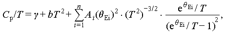 (4)
(4)
where the parameter γ refers to the electronic contribution. The formula bT2 is the Debye lattice contribution, in which the definition of parameter b is presented in Supplementary information. The last term represents the low-frequency phonon contribution, calculated by several localized Einstein-oscillator parameters, including numbers (n) and amplitudes (Ai) of the Einstein modes, and the Einstein temperature (θEi). Clearly, the experimental Cp results cannot be adequately fitted using a single Debye model or a Debye + 1Einstein model. However, it aligns well with the Debye + 2Einstein model, providing strong evidence for the occurrence of additional low-frequency optical phonons (Figure 6e, f). The relevant fitting results are presented in detail in Table S1. The θD derived from both heat capacity and phonon velocity, consistently shows a decreasing trend, experimentally validating that Ag alloying induces a significant acoustic-optical phonon coupling effect.
To elucidate the influence of acoustic-optical phonon coupling on the  of Cu1.85Ag0.15Sn0.9Cd0.1Se3, the spectral lattice thermal conductivity (κs) is calculated using the Debye-Callaway model. The formula is expressed as [40]
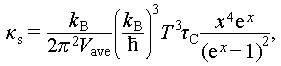 (5)
(5)
where x is defined by  , in which ω is the reduced phonon frequency. τc is the total phonon relaxation time, composed of several relaxation times including phonon-phonon Umklapp scattering (τU), grain boundary scattering (τB), point defect scattering (τP) and acoustic-optical phonon scattering (τAO). The τC can be given by [62]
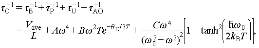
where L is the average grain size, constants A, B, and C are the fitted parameters, and ω0 is the optical phonon frequency obtained from the phonon dispersion curves. With the optimal fitting parameters (Table S2), the κs versus ω/ωD (ωD is the Debye frequency) for the Cu1.85Ag0.15Sn0.9Cd0.1Se3 is presented in Figure 6g. Clearly, under the influence of different scattering mechanisms, the  is effectively reduced, with a notable contribution from acoustic-optical (AO) phonon scattering. Consequently, the τc is also effectively suppressed by these scattering mechanisms (Figure 6h). A localized phonon frequency minimum of 7.1 THz is observed, resulting from the AO phonon overlap induced by Einstein oscillators. Therefore, phonons near this frequency are subjected to strong scattering, resulting in a sharp reduction in phonon relaxation time. Figure 6i depicts that these different scattering mechanisms reduce the
  across the entire temperature range, with AO phonon scattering playing a prominent role. The
  of Cu1.85Ag0.15Sn0.9Cd0.1Se3 is reduced by 22% due to point defect scattering, and further decreased by 46% as a result of AO phonon scattering.
Origin of acoustic-optical phonon coupling
The phonon dispersions and phonon density of states (PhDOS) for the pristine Cu2SnSe3 (Figure 7a), Cd-doped Cu2SnSe3 (Figure 7b), and Ag-alloyed Cu2SnSe3 (Figure 7c) were obtained by DFT calculations, providing a framework for analyzing the interactions between acoustic phonons and low-frequency optical phonons. Both Cd doping and Ag alloying introduce low-frequency optical phonons. However, Ag alloying is particularly notable for generating optical phonons at exceptionally low frequencies. The optical phonon mode at the Z point for Ag-alloyed Cu2SnSe3 exhibits a frequency as low as 18 cm−1, significantly lower than its Debye frequency (44 cm−1). Meanwhile, Ag alloying induces the most significant phonon softening, as evidenced by a Debye frequency of 44 cm−1, which is lower than that of Cd doping (51 cm−1) and the pristine Cu2SnSe3 (67 cm−1). The PhDOS further suggests that Ag atoms contribute to more low-frequency optical phonons (Figure S7). Additionally, both Cd doping and Ag alloying induce the “avoided-crossing” effect [64] between acoustic and optical phonons, resulting in changes in phonon dispersions and a significant reduction in phonon group velocity (Figure 7d). The acoustic-optical phonon coupling region is primarily centered within the low frequency ranges from 25 to 40 cm−1, and the heat carrier phonon scattering rate gradually increases with Cd doping and Ag alloying (Figure 7e). The average acoustic phonon scattering rates for pristine, Cd-doped, and Ag-alloyed Cu2SnSe3 are 0.068, 0.072, and 0.12 ps−1, respectively. The Grüneisen parameter shows a significant increase with Ag alloying, leading to pronounced anharmonic lattice vibrations among acoustic phonons. This results in a substantial drop in the  (Figure 7f). Significant differences in lattice anharmonicity have also been observed in other diamondoid compounds, such as (Cu, Ag)GaTe2 [49] and (Cu, Ag)InTe2 [65,66]. Eventually, both experimental and theoretical analyses consistently confirm that the ultra-low lattice thermal conductivity of Ag-alloyed Cu2SnSe3 (Figure S8) can be attributed to the strong scattering among these low-frequency acoustic-optical phonons.
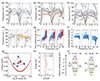 |
Figure 7 Origin of acoustic-optical phonon coupling in Cu2SnSe3. DFT-calculated phonon dispersions for (a) pristine, (b) Cd-doped, and (c) Ag-alloyed Cu2SnSe3. (d) Comparison of phonon dispersions along ΓX direction for pristine (left), Cd-doped (middle) and Ag-alloyed (right) Cu2SnSe3. The gradually softening transverse acoustic branches (TA and TA′) and longitudinal acoustic branch (LA) along with significant acoustic-optical coupling (red circles) are shown in the figure. (e) Comparison of total scattering rate within low-frequency phonons ranges for pristine (left), Cd-doped (middle) and Ag-alloyed (right) Cu2SnSe3. (f) Comparison of Grüneisen parameter for pristine (left), Cd-doped (middle) and Ag-alloyed (right) Cu2SnSe3, indicating the increased anharmonic lattice vibration from acoustic phonons. Energy profile of (g) Ag atom substituting Cu at different positions. The x = 0 suggests that the atom occupies the center of the Se tetrahedron; the calculated result shows that the off-centered Ag atoms displace 0.016 Å away from the center of the Se tetrahedron. (h) The crystal orbital Hamiltonian populations (COHP) are classified by different chemical bonds for Cu‒Se and Ag‒Se. (i) The schematic atomic orbital hybridization for Cu‒Se and Ag‒Se bonding, where the atomic orbital energy of Cu, Ag, and Se are obtained from NIST database LDA calculations [69]. The corresponding energy of bonding states is deduced from the atomic orbital energies. |
Our previous study indicated that Ag is off-centering in the tetrahedral coordination, which accounts for the AO phonon scattering and low  in Ag-based diamondoid materials. This off-centering behavior was not observed in the Cu2SnSe3 system. Therefore, it is crucial to investigate the local structure of Ag-alloyed Cu2SnSe3. The DFT calculations were performed to analyze the off-centered energy barrier of foreign atoms in Cu2SnSe3. Obviously, the system energy achieves a minimum when the Ag atom is displaced by 0.16 Å from its equilibrium position (Figure 7g). The off-centered atoms induce significant local tetrahedral distortions in the diamondoid lattice, suppressing both phonon velocity and average phonon free path [49]. To explore the underlying mechanism of the chemical bonding impacting the off-centered atoms, the crystal orbital Hamiltonian populations (COHP) were calculated for Ag-alloyed Cu2SnSe3. The calculated results indicate that the atomic bonding strength of Ag–Se is weaker than that of Cu–Se (Figure 7h). The integrated COHP (ICOHP) value for the Ag–Se bond is 3.10 eV, notably lower than the 4.07 eV value for the Cu–Se bond (Table S3). The decrease in ICOHP values indicates a weakening of chemical bonding, which leads to the pronounced Ag off-centering behavior. Furthermore, the nature of the weakened Ag–Se bond is described via an atomic orbital model of the Cu–Se and Ag–Se bonds (Figure 7i). In accordance with the valence-bond (VB) theory [67,68], for the I2-IV-VI3 diamondoid systems, Cu and Ag adopt sd3 hybridization, thereby establishing a stable tetrahedral coordination environment. A perfect diamondoid lattice requires a small energy difference between adjacent atomic orbitals, as a large energy gap could lead to a lower hybrid orbital state. However, the d-orbital energy of the Ag atom is significantly lower than that of the Cu atom. The large energy difference between the 4d and 5s orbitals of the Ag atom, leads to weaker sd3 hybridization. This explains the origin of local Ag atoms that deviate from the tetrahedral geometric center.
Comparison of thermoelectric performance
The Cd is an excellent dopant that can effectively enhance the electrical performance and reduce the  of Cu2SnSe3. Consequently, a ZTmax of 0.9 is obtained for the Cu2Sn0.94Cd0.06Se3 at 823 K. On the other hand, Ag alloying further improves the PF and significantly reduces the
  . Finally, a ZTmax of 1.3 at 800 K is obtained for the Cu1.85Ag0.15Sn0.9Cd0.1Se3. To further explore the power generation potential of Cu1.85Ag0.15Sn0.9Cd0.1Se3, we calculated its theoretical efficiency. When the temperature difference reaches 500 K, the theoretical efficiency is 6%. Additionally, We compare the ZT values of our material with other Cu2SnSe3-based compounds [40,41,46,70–72] (Figure 8). Our material exhibits the highest ZTmax at 800 K and achieves a decent average ZTave of 0.5 over the mid-temperature range (423–800 K), demonstrating the effectiveness of Cd doping and Ag alloying for improving the thermoelectric performance of Cu2SnSe3.
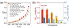 |
Figure 8 Comparison of thermoelectric performance for our sample with other Cu2SnSe3-based thermoelectrics. (a) Temperature dependence of ZT value for Cu2Sn0.94Cd0.06Se3, Cu1.85Ag0.15Sn0.9Cd0.1Se3, and other reported Cu2SnSe3-based thermoelectric systems. (b) Comparison of the maximum ZT (ZTmax) at 800 K and average ZT (ZTave) from 423‒800 K for this work and other Ag-optimized Cu2SnSe3 systems. |
CONCLUSIONS
Although diamondoid Cu2SnSe3 is considered a promising low-cost and ecofriendly thermoelectric material, its intrinsic monoclinic structure and compact packing of tetrahedral coordination lead to a light valence band structure and high intrinsic thermal conductivity, both hinder further improvement in its thermoelectric performance. In this study, we demonstrate the electron and phonon transport properties of Cu2SnSe3 can be significantly improved by carefully modifying its monoclinic structure into a distorted zinc blende cubic structure. We found the introduction of Cd promotes the crystal structural transition of Cu2SnSe3 from monoclinic to cubic, which reduces the deformation potential and enhances carrier mobility. Moreover, Cd doping not only simultaneously increases both carrier concentration and mobility, but also induces valence band convergence via the structural transition, significantly improving the density-of-states effective mass. As a result, Cd doping leads to an 870% improvement in the power factor of Cu2SnSe3. Furthermore, introducing the off-centering Ag distorts the Se4 tetrahedral structure, leading to local symmetry breaking in Cu2SnSe3. Our findings indicate that the off-centering Ag originates from the weakened sd3 orbital hybridization, which induces lattice softening and strong acoustic-optical phonon scattering. This suppression results in the lattice thermal conductivity to an extremely low value of 0.3 W m−1 K−1 at 800 K. Consequently, by combining the significantly improved electronic properties with the ultralow thermal conductivity, a high ZTmax of 1.3 at 800 K is achieved in Cu1.85Ag0.15Sn0.9Cd0.1Se3. This work provides a novel strategy to decouple the trade-off between carrier concentration, carrier mobility, and effective mass through deformation potential modification. Meanwhile, the Ag off-centering behavior and its influence on heat transport are studied systematically in the Cu2SnSe3 system. The present work demonstrates innovative strategies for further enhancing the thermoelectric performance of Cu2SnSe3 and other Cu-based diamondoid compounds.
MATERIALS AND METHODS
High-purity raw materials were weighed according to the corresponding stoichiometric ratios with a total weight of approximately 15 g and subsequently vacuum-sealed (10−2 Pa) in quartz crucibles. The sealed materials were then placed in a muffle furnace, where they were heated to 1273 K at a rate of 1.4 K min−1 and held at this temperature for 12 h. Following this, the samples were rapidly quenched to room temperature using cold water. The quenched specimens were then subjected to a 3 days ofannealing process at 723 K. After annealing, the ingots were densified using spark plasma sintering, employing a protocol that involved ramping up to 723 K within 7 min and holding at this temperature for 3 min under a vacuum of 10−1 Pa and a vertical pressure of 40 MPa. The sintered ingots were then sectioned into rectangular bars measuring 3 mm × 3 mm × 10 mm and square plates measuring 8 mm × 8 mm × 2 mm for evaluation of their electrical and thermal transport properties. The Seebeck coefficient was measured using the Cryoall CTA testing system, and the thermal diffusivity was assessed with the Cryoall CLA1000 system. Further details can be found in the Supplementary information.
Data availability
The original data are available from corresponding authors upon reasonable request.
Funding
This work was supported by the National Natural Science Foundation of China (52471217), the National Key Research and Development Program of China (2023YFB3809400), the National Science Fund for Distinguished Young Scholars (51925101), the Young Scientists Fund of the National Natural Science Foundation of China (52403348), the National Natural Science Foundation of China (52450001, 52250090, 52371208, 52002042, 51772012, 51571007 and 12374023), the Beijing Natural Science Foundation (JQ18004), and the Overseas Expertise Introduction Project for Discipline Innovation (111 Project) (B17002). L.-D.Z. appreciates the support from the Tencent Xplorer Prize.
Author contributions
P.C. performed the sample synthesis and thermoelectric transport property measurements. T.G., L.W. and S.Z. performed structural characterization. Y.W., Y.H. and X.G. performed the TEM analyses. H.H. and X.S. performed the Hall measurement. S.B. carried out the density functional theory calculations. Y.L., Z.Z., and D.G. performed the transport model fitting. All of the authors analyzed the data and discussed the underlying physics. P.C., H.X. and L.-D.Z. wrote the paper with contributions from the other authors. The manuscript reflects the contributions of all authors.
Conflict of interest
The authors declare no conflict of interest.
Supplementary information
Supplementary file provided by the authors. Access Supplementary Material
The supporting materials are published as submitted, without typesetting or editing. The responsibility for scientific accuracy and content remains entirely with the authors.
References
- Qin B, Kanatzidis MG, Zhao LD. The development and impact of tin selenide on thermoelectrics. Science 2024; 386: eadp2444. [Article] [CrossRef] [PubMed] [Google Scholar]
- Xiao Y, Zhao LD. Seeking new, highly effective thermoelectrics. Science 2020; 367: 1196-1197. [Article] [CrossRef] [PubMed] [Google Scholar]
- Shi XL, Zou J, Chen ZG. Advanced thermoelectric design: From materials and structures to devices. Chem Rev 2020; 120: 7399-7515. [Article] [Google Scholar]
- Xie H, Zhao L, Kanatzidis MG. Lattice dynamics and thermoelectric properties of diamondoid materials. Interdiscip Mater 2024; 3: 5-28. [Article] [Google Scholar]
- Xie H, Hao S, Cai S, et al. Ultralow thermal conductivity in diamondoid lattices: high thermoelectric performance in chalcopyrite Cu0.8+yAg0.2In1−yTe2. Energy Environ Sci 2020; 13: 3693-3705. [Article] [Google Scholar]
- Tang X, Li Z, Liu W, et al. A comprehensive review on Bi2Te3‐based thin films: Thermoelectrics and beyond. Interdiscip Mater 2022; 1: 88-115. [Article] [Google Scholar]
- Liu D, Wang D, Hong T, et al. Lattice plainification advances highly effective SnSe crystalline thermoelectrics. Science 2023; 380: 841-846. [Article] [Google Scholar]
- Qin Y, Qin B, Hong T, et al. Grid-plainification enables medium-temperature PbSe thermoelectrics to cool better than Bi2Te3. Science 2024; 383: 1204-1209. [Article] [Google Scholar]
- Liu S, Wen Y, Bai S, et al. Lattice plainification leads to high thermoelectric performance of p-type PbSe crystals. Adv Mater 2024; 36: 2401828. [Article] [CrossRef] [Google Scholar]
- Qin B, Wang D, Liu X, et al. Power generation and thermoelectric cooling enabled by momentum and energy multiband alignments. Science 2021; 373: 556-561. [Article] [Google Scholar]
- Jia B, Wu D, Xie L, et al. Pseudo-nanostructure and trapped-hole release induce high thermoelectric performance in PbTe. Science 2024; 384: 81-86. [Article] [NASA ADS] [CrossRef] [PubMed] [Google Scholar]
- Liu Y, Xie H, Li Z, et al. Unraveling the role of entropy in thermoelectrics: Entropy-stabilized quintuple rock salt PbGeSnCdxTe3+x. J Am Chem Soc 2023; 145: 8677-8688. [Article] [Google Scholar]
- Moshwan R, Shi XL, Liu WD, et al. Entropy engineering: An innovative strategy for designing high-performance thermoelectric materials and devices. Nano Today 2024; 58: 102475. [Article] [Google Scholar]
- Cai S, Hao S, Luo ZZ, et al. Discordant nature of Cd in PbSe: Off-centering and core–shell nanoscale CdSe precipitates lead to high thermoelectric performance. Energy Environ Sci 2020; 13: 200-211. [Article] [Google Scholar]
- Xie H, Zhao LD. Origin of off-centering effect and the influence on heat transport in thermoelectrics. Mater Futures 2024; 3: 013501. [Article] [Google Scholar]
- Li Y, Bai S, Wen Y, et al. Realizing high-efficiency thermoelectric module by suppressing donor-like effect and improving preferred orientation in n-type Bi2(Te, Se)3. Sci Bull 2024; 69: 1728-1737. [Article] [Google Scholar]
- Zhu YK, Sun Y, Dong X, et al. General design of high-performance and textured layered thermoelectric materials via stacking of mechanically exfoliated crystals. Joule 2024; 8: 2412-2424. [Article] [Google Scholar]
- Wang L, Wen Y, Bai S, et al. Realizing thermoelectric cooling and power generation in n-type PbS0.6Se0.4 via lattice plainification and interstitial doping. Nat Commun 2024; 15: 3782. [Article] [Google Scholar]
- Wang S, Wen Y, Bai S, et al. Realizing high-performance thermoelectric modules through enhancing the power factor via optimizing the carrier mobility in n-type PbSe crystals. Energy Environ Sci 2024; 17: 2588-2597. [Article] [Google Scholar]
- Zhan S, Bai S, Qiu Y, et al. Insight into carrier and phonon transports of PbSnS2 crystals. Adv Mater 2024; 36: 2412967. [Article] [CrossRef] [PubMed] [Google Scholar]
- Yuan W, Deng Q, Pan D, et al. Synergistic carrier and phonon transport advance Ag dynamically-doped n-type PbTe thermoelectrics via Mn alloying. J Mater Chem A 2024; 12: 1300-1308. [Article] [Google Scholar]
- Jin Y, Qiu Y, Bai S, et al. Modifying roles of CuSbSe2 in realizing high thermoelectric performance of GeTe. Adv Energy Mater 2024; 14: 2400623. [Article] [CrossRef] [Google Scholar]
- Li J, Zhang X, Wang X, et al. High-performance GeTe thermoelectrics in both rhombohedral and cubic phases. J Am Chem Soc 2018; 140: 16190-16197. [Article] [Google Scholar]
- Hong T, Qin B, Qin Y, et al. All-SnTe-based thermoelectric power generation enabled by stepwise optimization of n-type SnTe. J Am Chem Soc 2024; 146: 8727-8736. [Article] [Google Scholar]
- Ming H, Luo ZZ, Chen Z, et al. Chemical pressure-driven band convergence and discordant atoms intensify phonon scattering leading to high thermoelectric performance in SnTe. J Am Chem Soc 2024; 146: 28448-28458. [Article] [Google Scholar]
- Shi X, Song S, Gao G, et al. Global band convergence design for high-performance thermoelectric power generation in Zintls. Science 2024; 384: 757-762. [Article] [Google Scholar]
- Yin L, Li X, Bao X, et al. CALPHAD accelerated design of advanced full-Zintl thermoelectric device. Nat Commun 2024; 15: 1468. [Article] [Google Scholar]
- Qi Y, Lei H, Guo J, et al. Superconductivity in alkaline Earth metal-filled skutterudites BaxIr4X12 (X = As, P). J Am Chem Soc 2017; 139: 8106-8109. [Article] arxiv:1708.05166 [Google Scholar]
- Shi X, Yang J, Salvador JR, et al. Multiple-filled skutterudites: High thermoelectric figure of merit through separately optimizing electrical and thermal transports. J Am Chem Soc 2012; 134: 2842. [Article] [Google Scholar]
- Zhao LD, Lo SH, Zhang Y, et al. Ultralow thermal conductivity and high thermoelectric figure of merit in SnSe crystals. Nature 2014; 508: 373-377. [Article] [Google Scholar]
- Chang C, Wu M, He D, et al. 3D charge and 2D phonon transports leading to high out-of-plane ZT in n-type SnSe crystals. Science 2018; 360: 778-783. [Article] [Google Scholar]
- He W, Wang D, Wu H, et al. High thermoelectric performance in low-cost SnS0.91Se0.09 crystals. Science 2019; 365: 1418-1424. [Article] [Google Scholar]
- Hu Y, Bai S, Wen Y, et al. Stepwise optimization of thermoelectric performance in n-type SnS. Adv Funct Mater 2025; 35: 2414881. [Article] [CrossRef] [Google Scholar]
- Hu H, Ju Y, Yu J, et al. Highly stabilized and efficient thermoelectric copper selenide. Nat Mater 2024; 23: 527-534. [Article] [Google Scholar]
- Li JW, Han Z, Yu J, et al. Wide-temperature-range thermoelectric n-type Mg3(Sb, Bi)2 with high average and peak zT values. Nat Commun 2023; 14: 7428. [Article] [Google Scholar]
- Xie H, Liu Y, Zhang Y, et al. High thermoelectric performance in chalcopyrite Cu1−xAgxGaTe2–ZnTe: Nontrivial band structure and dynamic doping effect. J Am Chem Soc 2022; 144: 9113-9125. [Article] [Google Scholar]
- Xie H, Li Z, Liu Y, et al. Silver atom off-centering in diamondoid solid solutions causes crystallographic distortion and suppresses lattice thermal conductivity. J Am Chem Soc 2023; 145: 3211-3220. [Article] [Google Scholar]
- Zhang J, Liu R, Cheng N, et al. High‐performance pseudocubic thermoelectric materials from non-cubic chalcopyrite compounds. Adv Mater 2014; 26: 3848-3853. [Article] [Google Scholar]
- Qiu P, Qin Y, Zhang Q, et al. Intrinsically high thermoelectric performance in AgInSe2 n‐type diamond-like compounds. Adv Sci 2018; 5: 1700727. [Article] [Google Scholar]
- Ming H, Zhu C, Chen T, et al. Creating high-dense stacking faults and endo-grown nanoneedles to enhance phonon scattering and improve thermoelectric performance of Cu2SnSe3. Nano Energy 2022; 100: 107510. [Article] [Google Scholar]
- Hu L, Luo Y, Fang YW, et al. High thermoelectric performance through crystal symmetry enhancement in triply doped diamondoid compound Cu2SnSe3. Adv Energy Mater 2021; 11: 2100661. [Article] [CrossRef] [Google Scholar]
- Huang Y, Zhang B, Li J, et al. Unconventional doping effect leads to ultrahigh average thermoelectric power factor in Cu3SbSe4-based composites. Adv Mater 2022; 34: 2109952. [Article] [CrossRef] [PubMed] [Google Scholar]
- Nagaoka A, Yoshino K, Masuda T, et al. Environmentally friendly thermoelectric sulphide Cu2ZnSnS4 single crystals achieving a 1.6 dimensionless figure of merit ZT. J Mater Chem A 2021; 9: 15595-15604. [Article] [Google Scholar]
- Li W, Luo Y, Xu T, et al. Toward ultrahigh thermoelectric performance of Cu2SnS3‐based materials by analog alloying. Small 2023; 19: 2301963. [Article] [CrossRef] [PubMed] [Google Scholar]
- Marcano G, Rincón C, de Chalbaud LM, et al. Crystal growth and structure, electrical, and optical characterization of the semiconductor Cu2SnSe3. J Appl Phys 2001; 90: 1847-1853. [Article] [Google Scholar]
- Shi X, Xi L, Fan J, et al. Cu–Se bond network and thermoelectric compounds with complex diamondlike structure. Chem Mater 2010; 22: 6029-6031. [Article] [Google Scholar]
- Ming H, Zhu C, Chen T, et al. Theoretical study of intrinsic and extrinsic point defects and their effects on thermoelectric properties of Cu2SnSe3. Inorg Chem 2023; 62: 2607-2616. [Article] [Google Scholar]
- Yang X, Xu C, Giles NC. Intrinsic electron mobilities in CdSe, CdS, ZnO, and ZnS and their use in analysis of temperature-dependent Hall measurements. J Appl Phys 2008; 104: 073727. [Article] [CrossRef] [Google Scholar]
- Xie H, Bozin ES, Li Z, et al. Hidden local symmetry breaking in silver diamondoid compounds is root cause of ultralow thermal conductivity. Adv Mater 2022; 34: 2202255. [Article] [CrossRef] [PubMed] [Google Scholar]
- Skoug EJ, Cain JD, Morelli DT. Thermoelectric properties of the Cu2SnSe3–Cu2GeSe3 solid solution. J Alloys Compd 2010; 506: 18-21. [Article] [Google Scholar]
- Wang M, He M, Zhu L, et al. Boosting the thermoelectric performance of zinc blende-like Cu2SnSe3 through phase structure and band structure regulations. J Mater Chem A 2022; 10: 12946-12956. [Article] [Google Scholar]
- Ming H, Zhu G, Zhu C, et al. Boosting thermoelectric performance of Cu2SnSe3 via comprehensive band structure regulation and intensified phonon scattering by multidimensional defects. ACS Nano 2021; 15: 10532-10541. [Article] [Google Scholar]
- Gao D, Wen Y, Bai S, et al. Robustly boosting thermoelectric performance of n-type PbSe via lattice plainification and dynamic doping. Small 2024; 20: 2407556. [Article] [CrossRef] [PubMed] [Google Scholar]
- Shi H, Su L, Bai S, et al. Realizing high in-plane carrier mobility in n-type SnSe crystals through deformation potential modification. Energy Environ Sci 2023; 16: 3128-3136. [Article] [Google Scholar]
- Su L, Wang D, Wang S, et al. High thermoelectric performance realized through manipulating layered phonon-electron decoupling. Science 2022; 375: 1385-1389. [Article] [Google Scholar]
- Jin Y, Hong T, Wang D, et al. Band structure and microstructure modulations enable high quality factor to elevate thermoelectric performance in Ge0.9Sb0.1Te-x%FeTe2. Mater Today Phys 2021; 20: 100444. [Article] [Google Scholar]
- Lubchenko V, Wolynes PG. The origin of the boson peak and thermal conductivity plateau in low-temperature glasses. Proc Natl Acad Sci USA 2003; 100: 1515-1518. [Article] arxiv:cond-mat/0206194 [Google Scholar]
- Xu N, Wyart M, Liu AJ, et al. Excess vibrational modes and the boson peak in model glasses. Phys Rev Lett 2007; 98: 175502. [Article] arxiv:cond-mat/0611474 [CrossRef] [Google Scholar]
- Xie H, Su X, Hao S, et al. Large thermal conductivity drops in the diamondoid lattice of CuFeS2 by discordant atom doping. J Am Chem Soc 2019; 141: 18900-18909. [Article] [Google Scholar]
- Xie H, Su X, Zhang X, et al. Origin of intrinsically low thermal conductivity in talnakhite Cu17.6Fe17.6S32 thermoelectric material: Correlations between lattice dynamics and thermal transport. J Am Chem Soc 2019; 141: 10905-10914. [Article] [Google Scholar]
- Xie H, Hao S, Bao J, et al. All-inorganic halide perovskites as potential thermoelectric materials: Dynamic cation off-centering induces ultralow thermal conductivity. J Am Chem Soc 2020; 142: 9553-9563. [Article] [Google Scholar]
- Dong J, Liu Y, Li Z, et al. High thermoelectric performance in rhombohedral GeSe-LiBiTe2. J Am Chem Soc 2024; 146: 17355-17364. [Article] [Google Scholar]
- Wybourne MN, Kiff BJ. Acoustic-optical phonon scattering observed in the thermal conductivity of polydiacetylene single crystals. J Phys C-Solid State Phys 1985; 18: 309-318. [Article] [Google Scholar]
- Han S, Dai S, Ma J, et al. Strong phonon softening and avoided crossing in aliovalence-doped heavy-band thermoelectrics. Nat Phys 2023; 19: 1649-1657. [Article] arxiv:2303.10899 [Google Scholar]
- Liang HP, Geng S, Jia T, et al. Unveiling disparities and promises of Cu and Ag chalcopyrites for thermoelectrics. Phys Rev B 2024; 109: 035205. [Article] [CrossRef] [Google Scholar]
- Wang R, Cai J, Zhang Q, et al. Mismatched atomic bonds and ultralow thermal conductivity in Ag-based ternary chalcopyrites. Phys Rev B 2023; 107: 115202. [Article] [CrossRef] [Google Scholar]
- Frenking G, Fröhlich N. The nature of the bonding in transition-metal compounds. Chem Rev 2000; 100: 717-774. [Article] [Google Scholar]
- Root DM, Landis CR, Cleveland T. Valence bond concepts applied to the molecular mechanics description of molecular shapes. 1. Application to nonhypervalent molecules of the P-block. J Am Chem Soc 1993; 115: 4201-4209. [Article] [Google Scholar]
- Kotochigova S, Levine ZH, Shirley EL, et al. Local-density-functional calculations of the energy of atoms. Phys Rev A 1997; 55: 191-199. [Article] [Google Scholar]
- Fan YJ, Peng KL, Huang YL, et al. Enhanced thermoelectric performance of Cu2SnSe3 via synergistic effects of Cd-doping and CuGaTe2 alloying. Rare Met 2022; 41: 3466-3474. [Article] [Google Scholar]
- Li Y, Liu G, Cao T, et al. Enhanced thermoelectric properties of Cu2SnSe3 by (Ag, In)‐Co‐doping. Adv Funct Mater 2016; 26: 6025-6032. [Article] [Google Scholar]
- Zhou Y, Wu H, Wang D, et al. Investigations on electrical and thermal transport properties of Cu2SnSe3 with unusual coexisting nanophases. Mater Today Phys 2018; 7: 77-88. [Article] [Google Scholar]
All Figures
|
Figure 1 The optimization of thermoelectric performance for Cu2SnSe3. (a) Crystal structural transition from monoclinic to cubic due to Cd doping and the local tetrahedral distortion induced by Ag alloying. (b) Schematic diagram illustrating the simultaneous enhancement of carrier mobility and density-of-states effective mass by reducing the deformation potential (ξ) and promoting band convergence (Γ1V and Γ2V). (c) Schematic diagram illustrating the decrease in sound velocity (Vave) due to Ag off-centered behavior. (d) Comparison of carrier concentration (p), carrier mobility (μ), and effective mass (m*) between pristine Cu2SnSe3 and Cu2Sn0.9Cd0.1Se3. (e) Comparison of average sound velocity, Debye temperature (θD) and lattice thermal conductivity ( |
| In the text | |
|
Figure 2 Comparison of crystal structure and microstructure between monoclinic and cubic Cu2SnSe3. (a) XRD patterns of Cu2Sn1−xCdxSe3 (x varies from 0 to 0.15). The right panel shows an enlarged view of the main Bragg peak at 27°. (b) Lattice parameters as a function of x. (c), (d) Atomic-resolution HAADF images of pristine Cu2SnSe3. Corresponding SAD pattern taken along the [103] zone axis in (c); lattice model of the monoclinic structure in (d); atomic positions and distribution in (e). (f), (g) Atomic-resolution HAADF images of Cu2Sn0.9Cd0.1Se3. Corresponding SAD pattern taken along the [101] zone axis in (f); lattice model of the cubic structure in (g); atomic positions and distribution in (h). |
| In the text | |
|
Figure 3 Electronic properties and band structure of Cu2Sn1−xCdxSe3. (a) Room temperature Hall carrier concentration and Hall carrier mobility of Cu2Sn1−xCdxSe3. Temperature dependence of (b) electrical conductivity and (c) Seebeck coefficient of Cu2Sn1−xCdxSe3. Carrier concentration dependence of (d) Seebeck coefficient and (e) carrier mobility of Cu2Sn1−xCdxSe3, with the solid curve representing the theoretical prediction by the SPB model. The effective mass of the matrix is embedded within this figure. (f) Relative deformation potential as a function of carrier concentration. DFT-calculated electronic band structures for (g) monoclinic, (h) cubic and (i) Cd-doped cubic Cu2SnSe3. The decreased energy difference (∆E) at the VBM is presented in these figures. |
| In the text | |
|
Figure 4 Thermal conductivity and ZT value of Cu2Sn1−xCdxSe3. Temperature dependence of (a) power factor, (b) total thermal conductivity and lattice thermal conductivity, (c) ZT values and (d) quality factor B for the Cu2Sn1−xCdxSe3. |
| In the text | |
|
Figure 5 Thermoelectric performance of Cu2−yAgySn0.9Cd0.1Se3. (a) Room temperature Hall carrier concentration and Hall carrier mobility. Temperature dependence of (b) electrical conductivity, (c) Seebeck coefficient, (d) power factor, (e) total thermal conductivity and lattice thermal conductivity, and (f) ZT values. |
| In the text | |
|
Figure 6 Reduced lattice thermal conductivity due to strong acoustic-optical scattering. (a) Temperature dependence of lattice thermal conductivity for Cu2SnSe3, Cu2Sn0.9Cd0.1Se3 and Cu1.85Ag0.15Sn0.9Cd0.1Se3. (b) Room temperature sound velocity and (c) Debye temperature as a function of Ag content (y). (d) Low-temperature heat capacity for Cu2SnSe3, Cu2Sn0.9Cd0.1Se3, and Cu1.85Ag0.15Sn0.9Cd0.1Se3. (e) Relationship of Cp/T3 versus T for Cu1.85Ag0.15Sn0.9Cd0.1Se3 fitted with the Debye and Debye-Einstein models, respectively. (f) Relationship of Cp/T versus T2. The individual contributions from electronic (γ), Debye (β) and two Einsteins terms (E1, E2) are shown in the figure. (g) Spectral lattice thermal conductivity (κs), (h) phonon relaxation time (τc), and (i) lattice thermal conductivity for the Cu1.85Ag0.15Sn0.9Cd0.1Se3 fitted using the Debye-Callaway model. The contributions of Umklapp scattering (U), grain boundary scattering (B), point defect scattering (P), and acoustic-optical phonon scattering (AO) are calculated by the Debye-Callaway model. |
| In the text | |
|
Figure 7 Origin of acoustic-optical phonon coupling in Cu2SnSe3. DFT-calculated phonon dispersions for (a) pristine, (b) Cd-doped, and (c) Ag-alloyed Cu2SnSe3. (d) Comparison of phonon dispersions along ΓX direction for pristine (left), Cd-doped (middle) and Ag-alloyed (right) Cu2SnSe3. The gradually softening transverse acoustic branches (TA and TA′) and longitudinal acoustic branch (LA) along with significant acoustic-optical coupling (red circles) are shown in the figure. (e) Comparison of total scattering rate within low-frequency phonons ranges for pristine (left), Cd-doped (middle) and Ag-alloyed (right) Cu2SnSe3. (f) Comparison of Grüneisen parameter for pristine (left), Cd-doped (middle) and Ag-alloyed (right) Cu2SnSe3, indicating the increased anharmonic lattice vibration from acoustic phonons. Energy profile of (g) Ag atom substituting Cu at different positions. The x = 0 suggests that the atom occupies the center of the Se tetrahedron; the calculated result shows that the off-centered Ag atoms displace 0.016 Å away from the center of the Se tetrahedron. (h) The crystal orbital Hamiltonian populations (COHP) are classified by different chemical bonds for Cu‒Se and Ag‒Se. (i) The schematic atomic orbital hybridization for Cu‒Se and Ag‒Se bonding, where the atomic orbital energy of Cu, Ag, and Se are obtained from NIST database LDA calculations [69]. The corresponding energy of bonding states is deduced from the atomic orbital energies. |
| In the text | |
|
Figure 8 Comparison of thermoelectric performance for our sample with other Cu2SnSe3-based thermoelectrics. (a) Temperature dependence of ZT value for Cu2Sn0.94Cd0.06Se3, Cu1.85Ag0.15Sn0.9Cd0.1Se3, and other reported Cu2SnSe3-based thermoelectric systems. (b) Comparison of the maximum ZT (ZTmax) at 800 K and average ZT (ZTave) from 423‒800 K for this work and other Ag-optimized Cu2SnSe3 systems. |
| In the text | |
Current usage metrics show cumulative count of Article Views (full-text article views including HTML views, PDF and ePub downloads, according to the available data) and Abstracts Views on Vision4Press platform.
Data correspond to usage on the plateform after 2015. The current usage metrics is available 48-96 hours after online publication and is updated daily on week days.
Initial download of the metrics may take a while.