| Issue |
Natl Sci Open
Volume 4, Number 6, 2025
|
|
|---|---|---|
| Article Number | 20250059 | |
| Number of page(s) | 14 | |
| Section | Information Sciences | |
| DOI | https://doi.org/10.1360/nso/20250059 | |
| Published online | 06 November 2025 | |
RESEARCH ARTICLE
Ultrafast and stable flash memory with metal nanocrystals for logic-in-memory computing
1
State Key Laboratory of Integrated Chips and Systems, College of Integrated Circuits and Micro-Nano Electronics, Frontier Institute of Chip and System, Zhangjiang Fudan International Innovation Center, Fudan University, Shanghai 200433, China
2
Shaoxin Laboratory, Shaoxing 312035, China
* Corresponding authors (emails: This email address is being protected from spambots. You need JavaScript enabled to view it.
(Yang Wang); This email address is being protected from spambots. You need JavaScript enabled to view it.
(Chunsen Liu); This email address is being protected from spambots. You need JavaScript enabled to view it.
(Peng Zhou))
Received:
25
September
2025
Revised:
2
November
2025
Accepted:
4
November
2025
Abstract
Flash memory, the dominant non-volatile memory technology, is essential for data-driven computing systems. With the growing demands of the information age, there is an urgent need to enhance both its operational speed and data retention capabilities. Consequently, developing highly reliable memory that combines ultrafast write/erase operations with long-term retention has become a critical research objective. Here, we demonstrate a floating-gate memory based on a discrete Pt nanocrystal/h-BN/MoS2 van der Waals heterostructure, which combines ultrafast operation with long-term reliability. The Pt nanocrystals formed via rapid thermal annealing (RTA) are spatially isolated and effectively suppress charge leakage through tunneling defects, enabling stable device operation. The device exhibits excellent performance metrics, including a high on-off ratio (> 106), ultrafast operational speed (20 ns), impressive retention time (> 105 s), and good endurance (> 20,000 cycles). Furthermore, configurable logic-in-memory circuits are constructed, and a logic function is achieved by tuning the conductance of the FG memory.
Key words: flash memory / metal nanocrystals / van der Waals heterostructure / ultrafast operational speed / in-memory computing
© The Author(s) 2025. Published by Science Press and EDP Sciences.
 This is an Open Access article distributed under the terms of the Creative Commons Attribution License (https://creativecommons.org/licenses/by/4.0), which permits unrestricted use, distribution, and reproduction in any medium, provided the original work is properly cited.
INTRODUCTION
Memory has played a pivotal role in modern semiconductor industry in the rapid development of big data, artificial intelligence, and 5G communication technology. Since the invention of the floating gate memory by Bell Labs in 1967 [1], flash memory has occupied over 99% of the non-volatile memory market due to its low fabrication cost and high storage capacity [2]. Standard flash memory is basically a floating-gate (FG) metal-oxide-semiconductor transistor, which consists of a FG layer that is completely surrounded and electrically isolated by dielectrics, a blocking oxide layer, a tunneling layer, a channel layer and a capacitively coupled control gate [3]. However, the prevailing flash memory products in market typically operate at the speed in the range of microseconds [4,5], which hinders its application in high-performance systems. As the integration density of flash memory becomes higher, the thickness of tunneling layer scales accordingly, which cannot provide enough barrier to prevent leakage of charges in the FG layer [6]. Besides, electrons are able to move freely throughout a continuous metal floating gate that acts as the storage layer, and the leakage of the stored charges at different positions within the FG layer would possibly occur via defects in the tunneling layer [6,7], as illustrated in Figure 1(a). This would reduce the retention time of the device and hamper the non-volatile potential of the memory. At present, achieving ultrafast operating speed in the nanosecond range and stable data retention capability simultaneously remains a dominant challenge [8]. Therefore, it is crucial to explore new materials and structures to address the performance bottlenecks of silicon-based flash memories.
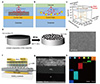 |
Figure 1 Nonvolatile flash memory embedded with Pt nanocrystals as the floating gate. (a), (b) The percolation model for gate leakage and comparison between continuous metal floating gate and metal nanocrystals floating gate in terms of charge leakage probability. (c) Comparison of speed, retention time, on/off ratio of 2D flash memory. (d) The formation process of Pt nanocrystals. A thin metal wetting layer of Pt deposited by EBE was transformed into nanocrystals by the RTA process. (e) SEM images of Pt nanocrystals. (f) Schematic structure diagram of the floating gate memory based on discrete Pt nanocrystals/h-BN/MoS2 van der Waals heterostructures. (g) A cross-sectional transmission electron microscope image of the device, highlighting the sharp and clean interfaces between different layers. (h) Elemental mapping image of the flash memory. |
In recent years, two-dimensional materials, such as graphene, hexagonal boron nitride (h-BN), and transition metal dichalcogenides (TMDs), have attracted wide attention and brought new opportunities for building the next generation of novel electronic devices [9–15]. Two-dimensionalal materials have atomically flat surfaces and ultrathin layers, and the absence of dangling bonds on surfaces can not only exhibit extraordinary electrical properties but also make it feasible to arbitrarily stack different layered structures to form van der Waals heterostructures without lattice mismatch [16–18]. Previously, it has been reported that two-dimensional flash memory can reduce the programming time to 20–30 ns [19–24]. However, these works barely focused on the improvement of the retention time and the endurance cycles. In addition, metal nanocrystals are widely adopted as charge trapping layers in the research of non-volatile memory due to their inherent advantages [25–27], including high density of states near the Fermi level, a wide range of work functions available, and strong coupling with substrate channels. The stored charges in discrete metal nanocrystals are isolated from each other by insulating dielectrics. Single charge leakage through defects in the tunneling layer would not cause the loss of all the charges in the floating gate, as shown in Figure 1(b), so metal-nanocrystal floating gate memory devices are endowed with better data retention characteristics compared to continuous metal floating gate memory. Although there is ample research focused on the development of novel and dependable memory devices, further exploration remains imperative to optimize memory performance in terms of high storage capacity, long retention, and significant endurance, and so on, as shown in Figure 1(c). Appropriate memory stack configurations and high-quality tunneling layers can significantly enhance programming speed and reduce leakage current, thereby improving data retention and endurance characteristics.
In this article, we report an ultrafast non-volatile memory utilizing the floating gate configuration based on the 2D van der Waals heterostructure and metal-nanocrystal storage layer, where the MoS2, h-BN, and Pt nanocrystals are served as the channel, tunneling, and floating gate materials. The proposed memory has a large memory window and exhibits distinguishable multilevel states by changing the pulse amplitude. The memory can operate at an ultrafast time of 20 ns and shows significant endurance up to 20,000 cycles. In addition, the memory has good retention characteristics exceeding 105 s at room temperature and a retention time of about 10 years is projected. Furthermore, inverters and NAND/NOR logic circuits based on the FG memory are demonstrated, in which logic operations can be directly performed using the memory elements. Our findings demonstrate a stable and robust flash memory and provide a possible route to in-memory computing architectures.
RESULTS AND DISCUSSION
Fabrication and characterization of flash memory
Metals with larger work functions form deeper potential wells, which can trap more charges and enhance retention without sacrificing injection efficiency [27]. Among numerous metal materials, platinum (Pt) has a large work function (5.65 eV) and can form deeper potential wells, resulting in better data retention properties after capturing charges. Figure 1(d) shows the scanning electron microscopy (SEM) images of Pt nanocrystals within a size range of 4–5 nm and a gap of a few nanometers, and the basic procedures for metal nanocrystal formation are illustrated in Figure 1(e). A thin metal wetting layer of Pt is evaporated by electron beam evaporation (EBE) followed by annealing at elevated temperatures close to its eutectic temperature to convert the metal film into nanocrystals [25,27]. During the RTA process, the film stress is relaxed and the surface energy is minimized. The elevated thermal energy enhances surface atom mobility so that the film self-assembles into a low-energy state. The nucleation and growth of nanocrystals is the process wherein non-equilibrium clusters reshape to achieve a locally stable energy state. Thermal activation during annealing facilitates the process by accelerating surface diffusion, enabling Pt atoms to assemble into structurally robust nanocrystals. The initial film thickness and RTA temperatures are important parameters for size control and distribution in nanocrystal formation. The nanocrystals formed under different conditions are presented in Figure S1. Notably, for the as-deposited Pt film with an initial thickness of a few nanometers, nanocrystals start to form prior to the RTA process. In addition, elevated temperatures induce crystalline phase transitions in the HfO2 lattice, producing grain boundary defects. These structural changes will trigger gate leakage currents and degrade device performance. Consequently, the RTA temperature for Pt films must be kept relatively low.
h-BN has a lower defect density and provides an atomically smooth surface free of dangling bonds and charge traps [18], which can strongly suppress and screen out the influence of defects in the tunneling layer on the charges stored in the floating gate. The selection principles for optimizing the thickness of h-BN tunneling layer involve two key requirements [20,24]: (1) to maximize the number of tunneling electrons to ensure efficient charge transfer, and (2) to suppress the reverse tunneling process to maintain stable retention. If the h-BN layer is excessively thin (< 7 nm), electrons would tunnel back to the channel after the voltage pulse is removed, which could severely deteriorate the retention characteristics. On the other hand, if the h-BN is too thick (> 15 nm), electrons would be difficult to tunnel through the barrier, leading to a decrease in the programming speed and a reduction in the storage capacity. Therefore, the thickness of h-BN in the ultrafast flash memory is found to be optimum at around 11 nm.
The schematic of the nonvolatile floating gate memory is illustrated in Figure 1(f), where a monolayer of MoS2 grown by chemical vapor deposition (CVD) acts as the channel, Pt nanocrystals serve as the floating gate, and a thick h-BN film (~11 nm) functions as the tunneling layer. A cross-sectional transmission electron microscopy (TEM) was conducted to thoroughly characterize interfaces between different functional components in the fabricated devices, which is presented in Figure 1(g). The results revealed atomically sharp and extremely clean interfaces between the different layers, free of gaps, defects and contamination. Energy-dispersive spectroscopy (EDS) mapping image further validated the compositional integrity of the heterostructure, as shown in Figure 1(h). Such high-quality interfaces achieved through precise fabrication are pivotal in enabling the exceptional device performance observed in our subsequent experiments. Details of the fabrication process are described in Section “Methods” and Figure S2. AFM images confirm the clean and flat surface of the bottom gate electrodes (Figure S3), which is essential for depositing a high-quality blocking layer and for minimizing the risk of dielectric breakdown. The effects of annealing in O2 atmosphere were characterized in Figure S4. The observed positive shift in threshold voltages demonstrates the passivation of oxygen vacancies within the HfO2 dielectric layer, which can enhance the quality of the blocking layer and improve device performance. The thickness of the h-BN flake was characterized by AFM, which was 11.5 nm, as shown in Figure S5.
Memory performance
In the memory stack configuration of HfO2/Pt nanocrystals/h-BN, the charges can be stored in Pt nanocrystals through the injection of electrons into the FG layer. The optical image of the nonvolatile flash memory is shown in Figure 2(a), where MoS2 and h-BN flakes are marked by yellow and white dashed lines, respectively. Figure 2(b) shows the transfer curve of the device under a gate voltage sweep with different ranges. The drain-source current (Ids) was acquired by sweeping the control gate voltage from negative to positive and then back to negative values while a drain-source bias (Vds) was kept constant at 100 mV. A sizable hysteresis was observed as the threshold voltage Vth can be regulated by the gate voltage pulse. The memory window is defined by the difference between the threshold voltages obtained from the forward and backward sweeps, which is a significant factor in identifying the information storage level. A large memory window is a critical prerequisite to distinguish the programmed and erased states [19]. When the control voltage gradually increases, the memory window becomes larger as more electrons tunnel into the floating gate. This suggests the significant regulation capability of the gate voltage on charge trapping in the floating gate. Notably, the device can be scanned back and forth without obvious hysteresis within a small range of the sweeping voltage, indicating a low charge trapping density at the interface. Meanwhile, the atomically sharp and defect-free interfaces between the channel and tunneling oxide layer result in ultralow leakage currents of 0.1 fA μm−1, as shown in Figure S6. The memory window and the on/off ratio are extracted from Figure 2(b) and are displayed in Figure 2(c) in linear scale and logarithmic scale, respectively.
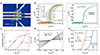 |
Figure 2 Structure and electrical properties of the Pt-nanocrystal floating gate memory. (a) Optical image of the nonvolatile flash memory. (b) Transfer curves of the flash memory. A distinct clockwise memory window expands as the back gate voltage increases from ±1 to ±10 V. No obvious hysteresis is observed within a small range of sweeping voltage, indicating negligible interface defect states. (c) Extracted ∆Vth and on-off ratio as a function of the maximum value of the gate voltage. (d) Output characteristic curves at different gate voltages. Vgs increases from 0 to 5 V in increments of 0.5 V. (e) The ultrafast programming test. States 0 and 1 can be achieved by applying a +23 V (20 ns) pulse and −28 V (20 ns) pulse, respectively. |
The amount of charge stored in the Pt nanocrystals can be calculated from the expression [20],

where e is the elementary charge of 1.6 × 10⁻¹⁹ C and Cblocking is the dielectric capacitance of high-k blocking layer HfO2, which is 1.475 μF cm−2. The density of stored electrons in FG layer is ≈ 5.32 × 1013 cm−2. Such a high charge density in the floating gate layer significantly surpasses that of conventional silicon-based flash memories [19].
We further fabricated a device consisting of MoS2 and h-BN layers to demonstrate the effect of the Pt nanocrystals floating gate on the memory window. Figure S7(b) shows that the memory window vanishes due to the absence of the floating gate. No hysteresis is observed in the transfer curve of the MoS2/h-BN FET in linear coordinates as depicted in Figure S7(c), which is attributed to the atomically clean surface of the h-BN layer. These findings underscore the essential role of the floating gate layer in producing large memory window [23,28] and enabling data storage capabilities.
Figure 2(d) presents the output characteristic curves of the memory device. The curves exhibit good linearity and symmetry for different gate voltages (Vgs ranging from 0 to 5 V with intervals of 0.5 V), indicating a high-quality ohmic contact between the channel material and the electrodes. Figure 2(e) demonstrates the ultrafast programming characteristics of the FG memory. The memory device can be toggled between state 0 and 1 by pulses of −28 V (20 ns) and 23 V (20 ns). The ultrafast voltage pulses are characterized by the oscilloscope and the waveforms are displayed in Figure S8.
To further understand the working mechanism of the nonvolatile memory, the energy band diagrams of the FG memory in different operation states are shown in Figure 3(a)−(d), and the flat band diagram is shown in Figure S9. The electron affinities of MoS2, h-BN and Pt are 4.2 [11], ≈ 2–2.3 [11], and 5.65 eV, respectively. The band gap of monolayer MoS2 and h-BN are 1.5 [29] and 5.96 eV [30], respectively, leading to potential barriers at the MoS2/h-BN interface of φe = 1.9–2.2 eV. The relative dielectric constants of HfO2 and h-BN are 25 and 3.5 [31], respectively, resulting in a high gate coupling ratio (GCR) of 0.84. The device achieves a small tunneling barrier and a large GCR through the structural design, which enhances the programming efficiency. When a positive voltage pulse is applied to the control gate, electrons in the MoS2 channel tunnel through the h-BN barrier into the Pt nanocrystals are trapped there. After the external electric field is turned off, the electrons trapped by the Pt nanocrystals cannot return to the MoS2 channel and are well retained due to the large potential barrier, completing the programming operation and resulting in a positive shift in the threshold voltage and thus high-resistance state of the MoS2 channel at Vgs = 0 V. This state is defined as the “program state”. Conversely, when applying a negative voltage pulse, the trapped electrons in the Pt nanocrystals can return back to the MoS2 channel, completing the erasing operation, inducing a negative shift in the threshold voltage and tuning the device to a high-conductance state after the negative gate voltage is removed. Consequently, the MoS2 channel exhibits low-resistance state at Vgs = 0 V, which is defined as the “erase state”. The basic device mechanism is rooted in the reported ultrafast 2D flash memory [19–22] and the nanocrystals floating gate enables optimized device performance.
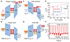 |
Figure 3 Program and erase operations of the flash memory with robust performance. (a)−(d) Energy band diagrams of the floating gate memory under positive and negative biases, corresponding to programming and erasing operations, respectively. (e) Endurance performance tested by a series of positive and negative pulses. The +22 V 50 ns/−24 V 50 ns pulses were used to repeatedly switch the memory between states 0 and 1. The drain current was read out at Vds = 100 mV, Vgs = 0 V. (f) The dynamic change of the channel current for multiple cycles after operations of 20,000 cycles. |
In addition, durability characteristics are important criteria of memory reliability. The robust endurance of our flash-memory device is demonstrated by repeatedly programming and erasing the memory cell as shown in Figure 3(e). The device can be switched back and forth between states 0 and 1 by applying alternate voltage pulses Vgs = 22 and −24 V for a duration of 50 ns to the control gate. The program and erase states remain distinguishable after operating for more than 20,000 cycles, indicating robust endurance and excellent stability. Following a series of programming cycles, the transfer curves were measured (Vds = 0.1 V) and Ids were extracted at Vgs = 0 V. The readout currents for state-0 and state-1 hardly shift suggesting well-suppressed stress in h-BN layer. The maximum endurance cycles of the flash memory are closely related to the stress-induced damage in the tunneling layer [24], as consecutive program and erase operations will generate defects and traps in h-BN layer. The dynamic change of memory states is displayed in Figure 3(f), exhibiting the stable and reproducible transition between the low- and high-resistance states. It should be noted that after 50,000 cycles of operation, the device still maintains normal transistor performance, as the gate leakage current remains low and the transfer curve exhibits on/off ratios over 105 (Figure S10(a), (b)). However, it is unable to perform erase and program operations due to the breakdown of the tunneling layer. As a result, the stored charge cannot be retained in the floating gate for extended periods, rendering the memory volatile. This can be proven by the variation of the channel current upon applying successive programming/erasing pulses shown in Figure S10(c). The current manifests transient changes triggered by the erase and program operations but it quickly returns to a steady state.
Data retention characteristics are essential measures of non-volatile memory. The device was first reset to original states and then erased and programmed by applying gate voltage pulses of –26 and +22 V with pulse widths of 50 ns, respectively. Subsequently, the changes in the threshold voltage over time were monitored in real-time by sweeping the transfer curves under room temperature conditions. The sweeping range is set to be relatively small, from –4 to 4 V, to minimize the effect of the measurements on the device’s state. As shown in Figure 4(a) and (b), the states 0 and 1 are almost unchanged over time, and the two current states can be stably maintained for more than 10,000 s with a large threshold voltage difference, indicating a low back-tunneling probability [24] as well as impressive retention characteristics. Figure 4(c) displays the time dependent channel currents at a fixed reading voltage of 0 V after programming and erasing operations, respectively. The current of the erase state changes from 100 to 30 nA while the program state shows almost no shift, demonstrating stable non-volatile retention characteristics. As indicated by the dashed line, the results project an 18% and 22% drop in the drain current of the program and erase states even after 10 years, respectively. Hence, a retention time of about 10 years can be estimated by the extrapolation method [32,33], making it feasible to realize long-term data retention at room temperature. In addition, we test the retention characteristics of the memory device again after 5 months and the channel current of program/erase states is still stably maintained for more than 105 s despite a faster decay. The experimental results confirm the highly reliable and robust data retention characteristics of the flash memory at room temperature.
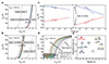 |
Figure 4 Retention performance of the ultrafast nonvolatile memory. (a) Transfer characteristic curves of the flash memory at different time intervals. The device was reset to state 1 and programmed to state 0 by a 22 V pulse with a 50 ns pulse width. (b) Transfer characteristic curves of the flash memory at different time intervals. The device was reset to state 0 and erased to state 1 by a −26 V pulse with a 50 ns pulse width. (c) Time variation of the channel current read at Vgs = 0 V. We expect that the device possesses the capability of a 10-year retention. After 5 months, the retention characteristics have been tested again. (d) The multibit storage of the nonvolatile flash memory. By applying a sequence of pulses with a duration of 50 ns and ranging from −18 to −27 V with steps of 1 V, transfer curves corresponding to the 10 states were obtained (black dashed line indicates the initial state-0). (e) Comparison of the operational speed and retention time of the reported memories. |
Multibit states operations
The high erasing/programming current ratio of our device enables multibit storage in a single memory cell [19], a capability critical for boosting data storage density and for applications such as in-memory computing. Figure 4(d) exemplifies the implementation of multilevel storage in our device, which is achieved by altering the amplitude of the gate voltage pulse. Before each erasing the memory was set to state 0 by a positive voltage pulse. Then a series of pulses with a duration of 50 ns and a progressive amplitude ranging from –18 to –27 V with intervals of 1 V were applied to the control gate. Following each programming pulse, transfer curves were measured and drain current was verified through a reading procedure at Vgs = 0 V and Vds = 0.1 V. The device was successfully erased to 10 distinguishable states as shown in Figure 4(d) and the time traces of the channel current are displayed in Figure S12, corresponding to 3-bit storage. The current values of different states remain stable and well-discernable, confirming the good multi-bit memory performance through electrical pulse modulation.
Combined with the atomically sharp interface properties of the MoS2/h-BN van der Waals heterostructures with the Pt nanocrystals with better immunities to charge leakage, our memory device manifests extraordinary performance compared with other floating gate memories based on 2D materials, as summarized in Table S1. Figure 4(e) illustrates the outstanding performance of our FG memory device in terms of speed and retention time. Note that our memory device occupies the corner with faster speed and longer retention time, providing an obvious performance advantage over other candidates [11,19,20,22,23,28,32–39]. The results provide a viable option for high-speed and robust nonvolatile memory applications and offer the ground for next-generation electronic devices based on 2D materials in the future.
Logic-in-memory operations based on the nonvolatile memory
By leveraging the electrically controllable multibit storage capability of the FG transistor, logic operations are executed [33,40]. Utilizing FG memory as the foundational building blocks enables the modulation of the threshold voltage, introducing an additional degree of freedom for applications in both digital and analogue circuits [32]. Inverters and logic circuits based on the nonvolatile memory are constructed. MoS2 transistor operating in saturation mode serves as the pull-up network while the FG transistor functions as the pull-down network. The width-to-length ratio (W/L) of both components is optimized to regulate the output voltage, ensuring the proper functionality of the circuits. The circuit diagrams and the detailed connections of the devices are presented in Figure 5(a), (b), (d), (e), (g), (h), while the fabrication processes are provided in Figure S13. The gate terminal of the FG memory serves dual functions: it can set the state of the memory by a voltage pulse and also acts as a terminal for applying the input voltage during logic operations. The logic inputs “0” and “1” correspond to positive and negative input voltage pulses, respectively, both with a duration of 50 ns. The output voltage of the circuit is defined as the logic output signal. The Vout is approximately 1 V at a Vdd of 1 V, which denotes logic “1”. On the contrary, a low output voltage value of nearly 0 V corresponds to logic “0”. The waveforms for the inverter, NAND, NOR logic operations are shown in Figure 5(c), (e), (f), respectively. For the inverter, when applying a positive pulse, the FG transistor is switched to a low conductance state. The pull-up transistor turns on, and the output voltage reaches Vdd. When a negative pulse is applied, the output reaches the ground and the pull-up transistor switches off. The output state remains stable after withdrawing each input voltage pulse due to the non-volatility of the FG memory. For NAND logic operations, the FG transistors operate in high resistance states under pulse configurations of IN-00, IN-01, and IN-10. A high output value of almost 1 V is obtained, corresponding to a logic “1”. When both inputs are negative pulses (IN-11), the Vout is nearly 0 V and the output signal is logic “0”. For NOR logic operations, the FG transistors are switched to low conductance states when both inputs are positive pulses (IN-00) and a high output voltage is measured. The Vout is approximately equal to 0 V when input pulses are IN-01, IN-10, and IN-11. Time traces show that the circuits are reproducible. The logic states are maintained because the operation results are stored in the FG transistor, proving the logic computing and data storage convergence of the in-situ memory and process circuit. The logic gates based on the FG memory are capable of executing the logic computing tasks as well as storing the output states, thereby demonstrating the in-memory logic paradigm [33,41]. Compared to conventional Boolean logic operations, the proposed logic-in-memory architecture demonstrates advantages in terms of transistor number reduction [42] and provides a solution to logic storage convergence, which opens a way to configure memory devices as key components of logic circuits.
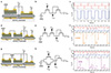 |
Figure 5 Logic-in-memory operations based on the nonvolatile flash memory. The output voltage is connected to the gate of the pull-up network, and the gates of flash memory are defined as the input terminals (positive voltage pulse as “0” and negative voltage pulse as “1”). (a) Schematic of the fabricated inverter logic device. (b) Circuit diagram of the inverter. (c) Operation of inverter logic with different input pulses. (d) Schematic of the fabricated NAND logic device. (e) Circuit diagram of the NAND device. (f) Operation of NAND logic with different input pulses. (g) Schematic of the fabricated NOR logic device. (h) Circuit diagram of the NOR device. (i) Operation of NOR logic with different input pulses. |
DISCUSSION
In this work, we proposed a FG memory device based on discrete Pt nanocrystals/h-BN/MoS2 van der Waals heterostructures, addressing the critical performance bottleneck inherent to conventional flash memory. The device demonstrates exceptional performance with a remarkable on-off ratio exceeding 106, ultrafast operational time of 20 ns, excellent endurance (> 20,000 cycles) and stable data retention (> 105 s). Moreover, the device exhibits a large memory window and multilevel nonvolatile storage with more than eight distinguishable states. Furthermore, inverters and NAND/NOR logic circuits based on the FG memory are realized, showing its potential for advanced logic-in-memory applications. Our floating gate memory paves the way for the next generation of high-performance non-volatile memory and will support in-memory computing systems in the future.
METHODS
Device fabrication
The bottom gate was first patterned by electron beam lithography (EBL), and then a 5/15 nm Cr/Pt stack was deposited by EBE on the silicon substrate with a 100 nm SiO2 thermal oxide layer. After the lift-off process, the metal gate was exposed to O2 plasma at 50 W for 20 s by reactive ion etching (RIE), followed by growing 15 nm HfO2 by atomic layer deposition (ALD). During the ALD process, tetrakis(ethylmethylamino)-hafnium reacts with water at 150°C to form HfO2. Annealing in O2 at 200°C for 1 h was carried out after ALD to fill the oxygen vacancies in the dielectric. A thin metal layer of Pt was deposited by EBE and was subsequently converted to discrete Pt nanocrystals by the rapid thermal annealing (RTA) process. Multilayer h-BN flake, with a thickness of ~12 nm, was mechanically exfoliated from bulk crystals by the Scotch tape method and transferred to the bottom gate electrode using a dry-transfer technique. The sample was then annealed in nitrogen atmosphere at 200°C for 2.5 h to remove tape residues and enhance adhesion to the substrate. Monolayer MoS2 grown by CVD was transferred onto the memory stack with a polystyrene-assisted transfer process. Next, MoS2 channels were patterned by EBL and etched into channel strips by O2 plasma. Finally, the source/drain electrodes (Cr/Au, 5 nm/40 nm) were defined by EBL and deposited by EBE.
Device characterization
The AFM images of the devices were scanned by an MFP-3D Origin+ (Asylum Research, Oxford Instruments) system. SEM images of the Pt nanocrystals were acquired by a JSM-7610F (JOEL) field emission SEM system under a 30 kV electron beam. TEM-ready samples were fabricated using an in situ focused ion beam (FIB) lift-out technique on a Thermo Scientific Helios Eurofins EAG lab G4 HX or UC Dual Beam FIB/SEM system. TEM images were acquired by a Thermo Scientific Tecnai F20 transmission electron microscope at an accelerating voltage of 200 kV. EDS images were obtained on the Super X FEI system under scanning transmission electron microscopy (STEM) mode. The electrical measurements of the FG memory device were performed at room temperature and under vacuum conditions in a probe station (PSM-VR-2S). The logic operations of the circuits were conducted under ambient conditions in a probe station (Cascade Summit 11000 type) at room temperature. The D.C. signals were generated using the source/monitor unit (SMU) in a B1500A semiconductor parameter analyzer (Keysight). For the ultrafast n/p programming test, voltage pulses were generated using the semiconductor pulse generator unit (SPGU) in the B1500A. The electrical characterization was conducted using the B1500A. For the endurance test, alternate positive and negative voltage pulses were generated by the SPGU in the B1500A, and the reading procedure was carried out by the SMU in the B1500A.
Funding
This work was supported by the National Key Research and Development Program of China (2024YFA1208400), the National Natural Science Foundation of China (62525401, 62322405, 62374042, 62090032 and 62304040), the Shanghai Pilot Program for Basic Research-Fudan University 21TQ1400100 (21TQ011), the New Cornerstone Science Foundation through the XPLORER PRIZE (62488101), the Young Scientist Project of the MOE Innovation Platform, and the Shaoxing Municipal Science and Technology Program Projects (2025A11016).
Author contributions
C.S.L., Y.W., and P.Z. conceived of the idea. C.H.L. designed and conducted the experiment. Y.J. and S.W. provided valuable assistance and discussion of the paper. C.H.L., Y.W., C.L., and P.Z. co-wrote the manuscript and all authors contributed to the discussion and revision of the manuscript.
Conflict of interest
The authors declare no conflict of interest.
Supplementary information
Supplementary file provided by the authors. Access Supplementary Material
References
- Kahng D, Sze SM. A floating gate and its application to memory devices. Bell Syst Tech J 1967; 46: 1288-1295. [Article] [Google Scholar]
- IEEE. IRDSTM Roadmap. https://irds.ieee.org/editions [Google Scholar]
- Bez R, Camerlenghi E, Modelli A, et al. Introduction to flash memory. Proc IEEE 2003; 91: 489-502. [Article] [Google Scholar]
- Cho W, Jeong C, Kim J, et al. A 321-layer 2Tb 4b/cell 3D-NAND-flash memory with a 75MB/s program throughput. In: Proceedings of the 2025 IEEE International Solid-State Circuits Conference (ISSCC). San Francisco, 2025, 512–514 [Google Scholar]
- Jung W, Kim H, Kim DB, et al. 13.3 A 280-layer 1Tb 4b/cell 3D-NAND flash memory with a 28.5Gb/mm2 areal density and a 3.2GB/s high-speed IO rate. In: Proceedings of the 2024 IEEE International Solid-State Circuits Conference (ISSCC). San Francisco, 2024, 236–237 [Google Scholar]
- Lu CY. Future prospects of NAND flash memory technology—The evolution from floating gate to charge trapping to 3d stacking. J Nanosci Nanotech 2012; 12: 7604-7618. [Article] [Google Scholar]
- Rajput R, Vaid R. Flash memory devices with metal floating gate/metal nanocrystals as the charge storage layer: A status review. Facta Univ Electron Energ 2020; 33: 155-167. [Article] [Google Scholar]
- Jeong J, Song Y, Hahn SS, et al. Dynamic erase voltage and time scaling for extending lifetime of NAND flash-based SSDs. IEEE Trans Comput 2017; 66: 616-630. [Article] [Google Scholar]
- Chen ML, Sun X, Liu H, et al. A FinFET with one atomic layer channel. Nat Commun 2020; 11: 1205. [Article] [Google Scholar]
- Jiang J, Xu L, Qiu C, et al. Ballistic two-dimensional InSe transistors. Nature 2023; 616: 470-475. [Article] [Google Scholar]
- Sup Choi M, Lee GH, Yu YJ, et al. Controlled charge trapping by molybdenum disulphide and graphene in ultrathin heterostructured memory devices. Nat Commun 2013; 4: 1624. [Article] [Google Scholar]
- Desai SB, Madhvapathy SR, Sachid AB, et al. MoS2 transistors with 1-nanometer gate lengths. Science 2016; 354: 99-102. [Article] [Google Scholar]
- Bertolazzi S, Krasnozhon D, Kis A. Nonvolatile memory cells based on MoS2/graphene heterostructures. ACS Nano 2013; 7: 3246-3252. [Article] [Google Scholar]
- Radisavljevic B, Radenovic A, Brivio J, et al. Single-layer MoS2 transistors. Nat Nanotech 2011; 6: 147-150. [Article] [NASA ADS] [CrossRef] [PubMed] [Google Scholar]
- Wu F, Tian H, Shen Y, et al. Vertical MoS2 transistors with sub-1-nm gate lengths. Nature 2022; 603: 259-264. [Article] [CrossRef] [PubMed] [Google Scholar]
- Geim AK, Grigorieva IV. Van der Waals heterostructures. Nature 2013; 499: 419-425. [Article] [NASA ADS] [CrossRef] [PubMed] [Google Scholar]
- Liu Y, Weiss NO, Duan X, et al. Van der Waals heterostructures and devices. Nat Rev Mater 2016; 1: 16042. [Article] [Google Scholar]
- Novoselov KS, Mishchenko A, Carvalho A, et al. 2D materials and van der Waals heterostructures. Science 2016; 353: aac9439. [Article] [Google Scholar]
- Wu L, Wang A, Shi J, et al. Atomically sharp interface enabled ultrahigh-speed non-volatile memory devices. Nat Nanotech 2021; 16: 882-887. [Article] [Google Scholar]
- Liu L, Liu C, Jiang L, et al. Ultrafast non-volatile flash memory based on van der Waals heterostructures. Nat Nanotech 2021; 16: 874-881. [Article] [Google Scholar]
- Huang X, Liu C, Tang Z, et al. An ultrafast bipolar flash memory for self-activated in-memory computing. Nat Nanotech 2023; 18: 486-492. [Article] [Google Scholar]
- Jiang Y, Liu C, Cao Z, et al. A scalable integration process for ultrafast two-dimensional flash memory. Nat Electron 2024; 7: 868-875. [Article] [Google Scholar]
- Lu H, Wang Y, Han X, et al. An ultrafast multibit memory based on the ReS2/h-BN/graphene heterostructure. ACS Nano 2024; 18: 23403-23411. [Article] [Google Scholar]
- Wang H, Guo H, Guzman R, et al. Ultrafast non-volatile floating-gate memory based on all-2D materials. Adv Mater 2024; 36: 2311652. [Article] [Google Scholar]
- Liu Z, Lee C, Narayanan V, et al. Metal nanocrystal memories. I. Device design and fabrication. IEEE Trans Electron Devices 2002; 49: 1606-1613. [Article] [Google Scholar]
- Wang J, Zou X, Xiao X, et al. Floating gate memory-based monolayer MoS2 transistor with metal nanocrystals embedded in the gate dielectrics. Small 2015; 11: 208-213. [Article] [Google Scholar]
- Lee C, Meteer J, Narayanan V, et al. Self-assembly of metal nanocrystals on ultrathin oxide for nonvolatile memory applications. J Elec Materi 2005; 34: 1-11. [Article] [Google Scholar]
- Bach TPA, Cho S, Kim H, et al. 2D van der Waals heterostructure with tellurene floating-gate for wide range and multi-bit optoelectronic memory. ACS Nano 2024; 18: 4131-4139. [Article] [Google Scholar]
- Shen PC, Su C, Lin Y, et al. Ultralow contact resistance between semimetal and monolayer semiconductors. Nature 2021; 593: 211-217. [Article] [NASA ADS] [CrossRef] [PubMed] [Google Scholar]
- Cassabois G, Valvin P, Gil B. Hexagonal boron nitride is an indirect bandgap semiconductor. Nat Photon 2016; 10: 262-266. [Article] [Google Scholar]
- Zhang C, Tu T, Wang J, et al. Single-crystalline van der Waals layered dielectric with high dielectric constant. Nat Mater 2023; 22: 832-837. [Article] [Google Scholar]
- Migliato Marega G, Zhao Y, Avsar A, et al. Logic-in-memory based on an atomically thin semiconductor. Nature 2020; 587: 72-77. [Article] [NASA ADS] [CrossRef] [PubMed] [Google Scholar]
- Niu W, Zou X, Tang L, et al. Van der Waals gap enabled robust retention of MoS2 floating-gate memory for logic-in-memory operations. Adv Funct Mater 2025; 35: 2422120. [Article] [Google Scholar]
- Kim YK, Park S, Choi J, et al. Low-power charge trap flash memory with MoS2 channel for high-density in-memory computing. Adv Funct Mater 2024; 34: 2405670. [Article] [Google Scholar]
- Migliato Marega G, Ji HG, Wang Z, et al. A large-scale integrated vector-matrix multiplication processor based on monolayer molybdenum disulfide memories. Nat Electron 2023; 6: 991-998. [Article] [Google Scholar]
- Migliato Marega G, Wang Z, Paliy M, et al. Low-power artificial neural network perceptron based on monolayer MoS2. ACS Nano 2022; 16: 3684-3694. [Article] [Google Scholar]
- Cai Y, Yang J, Hou Y, et al. 8-bit states in 2D floating-gate memories using gate-injection mode for large-scale convolutional neural networks. Nat Commun 2025; 16: 2649. [Article] [Google Scholar]
- Wang W, Jin J, Wang Y, et al. High-speed optoelectronic nonvolatile memory based on van der Waals heterostructures. Small 2023; 19: 2304730. [Article] [Google Scholar]
- Zha J, Xia Y, Shi S, et al. A 2D heterostructure-based multifunctional floating gate memory device for multimodal reservoir computing. Adv Mater 2024; 36: 2308502. [Article] [Google Scholar]
- Mukherjee B, Zulkefli A, Watanabe K, et al. Laser-assisted multilevel non-volatile memory device based on 2D van-der-Waals few-layer-ReS2/h-BN/graphene heterostructures. Adv Funct Mater 2020; 30: 2001688. [Article] [Google Scholar]
- Liu C, Chen H, Hou X, et al. Small footprint transistor architecture for photoswitching logic and in situ memory. Nat Nanotech 2019; 14: 662-667. [Article] [Google Scholar]
- Liao J, Wen W, Wu J, et al. Van der Waals ferroelectric semiconductor field effect transistor for in-memory computing. ACS Nano 2023; 17: 6095-6102. [Article] [Google Scholar]
All Figures
|
Figure 1 Nonvolatile flash memory embedded with Pt nanocrystals as the floating gate. (a), (b) The percolation model for gate leakage and comparison between continuous metal floating gate and metal nanocrystals floating gate in terms of charge leakage probability. (c) Comparison of speed, retention time, on/off ratio of 2D flash memory. (d) The formation process of Pt nanocrystals. A thin metal wetting layer of Pt deposited by EBE was transformed into nanocrystals by the RTA process. (e) SEM images of Pt nanocrystals. (f) Schematic structure diagram of the floating gate memory based on discrete Pt nanocrystals/h-BN/MoS2 van der Waals heterostructures. (g) A cross-sectional transmission electron microscope image of the device, highlighting the sharp and clean interfaces between different layers. (h) Elemental mapping image of the flash memory. |
| In the text | |
|
Figure 2 Structure and electrical properties of the Pt-nanocrystal floating gate memory. (a) Optical image of the nonvolatile flash memory. (b) Transfer curves of the flash memory. A distinct clockwise memory window expands as the back gate voltage increases from ±1 to ±10 V. No obvious hysteresis is observed within a small range of sweeping voltage, indicating negligible interface defect states. (c) Extracted ∆Vth and on-off ratio as a function of the maximum value of the gate voltage. (d) Output characteristic curves at different gate voltages. Vgs increases from 0 to 5 V in increments of 0.5 V. (e) The ultrafast programming test. States 0 and 1 can be achieved by applying a +23 V (20 ns) pulse and −28 V (20 ns) pulse, respectively. |
| In the text | |
|
Figure 3 Program and erase operations of the flash memory with robust performance. (a)−(d) Energy band diagrams of the floating gate memory under positive and negative biases, corresponding to programming and erasing operations, respectively. (e) Endurance performance tested by a series of positive and negative pulses. The +22 V 50 ns/−24 V 50 ns pulses were used to repeatedly switch the memory between states 0 and 1. The drain current was read out at Vds = 100 mV, Vgs = 0 V. (f) The dynamic change of the channel current for multiple cycles after operations of 20,000 cycles. |
| In the text | |
|
Figure 4 Retention performance of the ultrafast nonvolatile memory. (a) Transfer characteristic curves of the flash memory at different time intervals. The device was reset to state 1 and programmed to state 0 by a 22 V pulse with a 50 ns pulse width. (b) Transfer characteristic curves of the flash memory at different time intervals. The device was reset to state 0 and erased to state 1 by a −26 V pulse with a 50 ns pulse width. (c) Time variation of the channel current read at Vgs = 0 V. We expect that the device possesses the capability of a 10-year retention. After 5 months, the retention characteristics have been tested again. (d) The multibit storage of the nonvolatile flash memory. By applying a sequence of pulses with a duration of 50 ns and ranging from −18 to −27 V with steps of 1 V, transfer curves corresponding to the 10 states were obtained (black dashed line indicates the initial state-0). (e) Comparison of the operational speed and retention time of the reported memories. |
| In the text | |
|
Figure 5 Logic-in-memory operations based on the nonvolatile flash memory. The output voltage is connected to the gate of the pull-up network, and the gates of flash memory are defined as the input terminals (positive voltage pulse as “0” and negative voltage pulse as “1”). (a) Schematic of the fabricated inverter logic device. (b) Circuit diagram of the inverter. (c) Operation of inverter logic with different input pulses. (d) Schematic of the fabricated NAND logic device. (e) Circuit diagram of the NAND device. (f) Operation of NAND logic with different input pulses. (g) Schematic of the fabricated NOR logic device. (h) Circuit diagram of the NOR device. (i) Operation of NOR logic with different input pulses. |
| In the text | |
Current usage metrics show cumulative count of Article Views (full-text article views including HTML views, PDF and ePub downloads, according to the available data) and Abstracts Views on Vision4Press platform.
Data correspond to usage on the plateform after 2015. The current usage metrics is available 48-96 hours after online publication and is updated daily on week days.
Initial download of the metrics may take a while.